


xilinx FPGA jesd204b ADC篇(0):JESD204术语-优快云博客
xilinx FPGA jesd204b ADC篇(1):什么是JESD204-优快云博客
xilinx FPGA jesd204b ADC篇(2):JESD204的意义-优快云博客
xilinx FPGA jesd204b ADC篇(3):高速数据转换器的输出接口-优快云博客
xilinx FPGA jesd204b ADC篇(4):JESD204B接口介绍-优快云博客
xilinx FPGA jesd204b ADC篇(5):JESD204B接口的关键-优快云博客
xilinx FPGA jesd204b ADC篇(6):JESD204B IP核简介-优快云博客
xilinx FPGA jesd204b ADC篇(7):JESD204B IP核端口介绍-优快云博客
xilinx FPGA jesd204b ADC篇(8):JESD204B IP核寄存器-优快云博客
xilinx FPGA jesd204b ADC篇(9):JESD204B IP核设计实现-优快云博客
xilinx FPGA jesd204b ADC篇(10):JESD204B IP核的AXI4-lite配置接口读写-优快云博客
xilinx FPGA jesd204b ADC篇(11):JESD204B ADC硬件实现架构-优快云博客
xilinx FPGA jesd204b ADC篇(12):JESD204B ADC数据采集实现-优快云博客
*******私信博主请加V:FPGA_GO*******
博主小飞继续和大家分享xilinx FPGA jesd204b ADC篇的第10部分相关内容~
本篇咱们介绍jesd204b ip核的AXI4-Lite配置接口的数据读写操作。如下表所示为AXI4-Lite协议所使用信号的官方标准,共有21组信号:

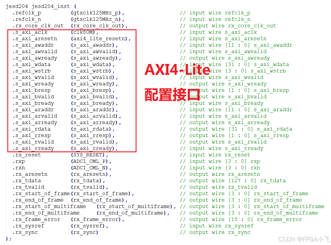
如下图所示为vivado例化的JESD204 IP核,其中标记部分即为AXI4-Lite接口,共有19组信号,官方标准中的AWPROT和ARPROT信号无需使用。操作这19组信号即可实现对JESD204 IP核的寄存器配置与状态监测,小飞接下来详细介绍这些信号:
全局信号:
1)s_axi_aclk
接口的读写时钟,默认为100MHz,由用户提供。
2)s_axi_aresetn
接口的复位信号,默认低电平复位,由用户提供,最好使用同步复位。
| Table A2-1 Global signals | ||
| Signal | source | description |
| ACLK | Clock source | Global clock signal |
| ARESETn | Reset source | Global reset signal, active LOW |
| All signals are sampled on the rising edge of the global clock | ||
写地址信号:
1)s_axi_awaddr
写地址信号。用户向IP核发送12bit位宽的寄存器地址信号,准备向该地址写入数据。
2)s_axi_awvalid
写地址可用信号。用户向IP核发送1bit位宽的写地址可用信号,告诉IP核,用户端发送的12bit地址是有效的。
3)s_axi_awready
写地址准备信号。IP核向用户端发送1bit位宽的写地址准备信号,告诉用户端,它已经准备好接收12bit的寄存器地址信号了。
| Table A2-2 Write address channel signals | ||
| Signal | source | description |
| AWADDR | Master | Write address. The write address gives the address of the first transfer in a write burst transaction |
| AWVALID | Master | Write address valid. This signal indicates that the channel is signaling valid write address and control information |
| AWREADY | Slave | Write address ready. This signal indicates that the slave is ready to accept an address and associated control signal |
写数据信号:
1)s_axi_wdata
写数据信号。用户向IP核写入32bit位宽的寄存器配置数据,写入的地址即为上表中的12bit位宽的地址。
2)s_axi_wstrb
写字节有效信号。该信号4bit位宽,每bit信号标志着8bit的写入数据是否有效。4bit位宽的该信号正好对应32bit的写数据信号是否有效。用户在向IP核写入32bit的 s_axi_wdata时,同时要写入s_axi_wstrb,一般s_axi_wstrb置为全1即可,表明写入数据都是可用的。
3)s_axi_wvalid
写可用信号。用户向IP核发送该信号,表明s_axi_wdata和s_axi_wstrb信号对于IP核都是可用的。
4)s_axi_wready
写准备信号。IP核向用户发送该信号,表明IP核已经准备好接收来自用户端的s_axi_wdata和s_axi_wstrb信号。
| Table A2-3 Write data channel signals | ||
| Signal | source | description |
| WDATA | Master | Write data |
| WSTRB | Master | Write strobes. This signal indicates which byte lanes hold valid data. There is one write strobe bit for each eight bits of the write data bus |
| WVALID | Master | Write valid. This signal indicates that valid write data and strobes are available |
| WREADY | Slave | Write ready. This signal indicates that the slave can accept the write data |
写响应信号:
1)s_axi_bresp
写响应信号。该信号2bit位宽,当用户向IP核写入数据后,IP核会向用户反馈写入是否成功。s_axi_bresp共4种状态,当其为2’b00时,表示写成功。
2)s_axi_bvalid
写响应可用信号。该信号1bit位宽,表示此时写响应信号可用,在该标志位下,用户获取写响应信号,此信号由IP核提供,用户端接收。
3)s_axi_bready
写响应准备信号。该信号1bit位宽,由用户端发送到IP核,表示用户端已经准备好接收s_axi_bresp和s_axi_bvalid信号。
| Table A2-4 Write response channel signals | ||
| Signal | source | description |
| BRESP | Slave | Write response. This signal indicates the status of the write transaction |
| BVALID | Slave | Write response valid. This signal indicates that the channel is signaling a valid write response |
| BREADY | Master | Response ready. This signal indicates that the master can accept a write response to accept an address and associated control signal |
读地址信号:
1)s_axi_araddr
读地址信号。用户向IP核写入需要读写的寄存器地址,共12bit位宽。
2)s_axi_arvalid
读地址可用信号。用户向IP核提供读地址可用信号,共1bit位宽,该标志位与s_axi_araddr信号同时发送到IP核。
3)s_axi_arready
写地址准备信号。IP核向用户提供该1bit位宽信号,来告诉用户什么时候可以向它写入s_axi_araddr和s_axi_arvalid信号
| Table A2-5 Read address channel signals | ||
| Signal | source | description |
| ARADDR | Master | Read address. The read address gives the address of the first transfer in a read burst transaction |
| ARVALID | Master | Read address valid. This signal indicates that the channel is signaling valid read address and control information |
| ARREADY | Slave | Read address ready. This signal indicates that the slave is ready to accept an address and associated control signals |
读数据信号:
1)s_axi_rdata
读数据信号。该信号32bit位宽,由IP核提供给用户,是寄存器的值。
2)s_axi_rresp
读数据响应。IP核向用户传输寄存器值时,还同时传输该响应信号,该信号2bit位宽,指示读数据的共4种状态,其中2’b00表示正常。
3)s_axi_rvalid
读数据可用信号。该信号作为读数据信号的可用标志信号,同样由IP核提供给用户。
4)s_axi_rready
读数据准备信号。用户向IP提供该1bit信号,表示用户端已经准备好接收数据了。
| Table A2-6 Read data channel signals | ||
| Signal | source | description |
| RDATA | Slave | Read data |
| RRESP | Slave | Read response. This signal indicates the status of the read transfer |
| RVALID | Slave | Read valid. This signal indicates that the channel is signaling the required read data |
| RREADY | Master | Read ready. This signal indicates that the master can accept the read data and response information |
AXI4-Lite协议所使用的信号在这里就介绍完毕了,接下来小飞具体介绍实现该协议的重要时序关系~
写时序
如下图所示为AXI4-lite写逻辑的时序图,仅供参考。通俗的说:如果咱们想配置JESD204 IP核,就必须按照如下图的时序关系才能实现。实现步骤可以分为3步:写地址、写数据以及写响应。
1)写地址
当监测到IP核给出的AWREADY有效时,用户在时钟上升沿写入寄存器数据的地址AWADDR以及地址使能AWVALID。
2)写数据
当监测到WREADY有效时,用户在时钟上升沿写入寄存器数据WDATA、WSTRB以及数据使能WVALID。
3)写响应
当监测到BREADY、BVALID均有效时,用户获取写响应信号BRESP。

读时序
如下图所示为AXI4-lite读逻辑的时序图,仅供参考。如果咱们想读取JESD204 IP核的内部寄存器值,就必须按照如图的时序关系才能实现。实现步骤可以分为2步:写地址、读数据以及读响应。
1)写地址
当监测到IP核给出的ARREADY有效时,用户在时钟上升沿写入寄存器数据的地址ARADDR以及地址使能ARVALID。
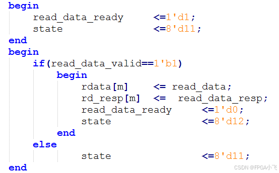
2)读数据及读响应
当监测到IP核给出的RVALID有效且用户端的RREADY有效时,用户在时钟上升沿读取寄存器数据RDATA以及读响应信号RRESP。

下面博主小飞给大家分享FPGA读写AXI4-lite时序的verilog核心代码~
写地址逻辑:

写数据逻辑:

写响应逻辑:

读操作的写地址逻辑:

读数据及读响应:
测试结果展示
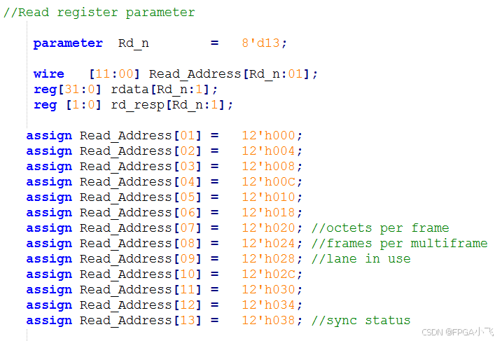
博主小飞在该测试演示中配置了JESD204 IP核的11个关键寄存器,如下图代码所示:

配置完成后,再将13个寄存器的值读出来:
用逻辑分析仪可以看到,写入的数据和读出的数据是完全相同的,证明AXI4-Lite接口的读写时序没问题~


 5627
5627

 被折叠的 条评论
为什么被折叠?
被折叠的 条评论
为什么被折叠?
 到【灌水乐园】发言


