


 本文详细介绍了数字系统设计中的各种触发器实现方法,包括基本的D触发器、带同步复位的D触发器、16位D触发器、锁存器、JK触发器以及脉冲边沿检测等高级应用。同时探讨了这些触发器如何用于信号检测和状态维护。
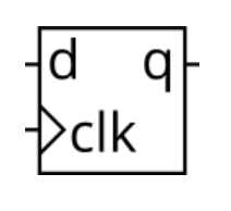
D触发器:
module top_module (
    input clk,    // Clocks are used in sequential circuits
    input d,
    output reg q );//
    always @(posedge clk) begin
         q<=d;
    end
    // Use a clocked always block
    //   copy d to q at every positive edge of clk
    //   Clocked always blocks should use non-blocking assignments

endmodule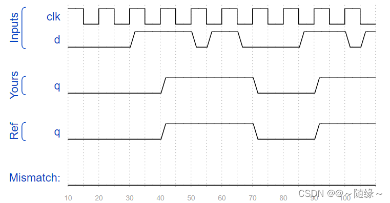
加reset:
Create 8 D flip-flops with active high synchronous reset. All DFFs should be triggered by the positive edge of clk.
module top_module (
    input clk,
    input reset,            // Synchronous reset
    input [7:0] d,
    output [7:0] q
);
    always @(posedge clk) begin
        if(!reset)
            q<=d;
        else
            q<=1'b0;
    end
endmodule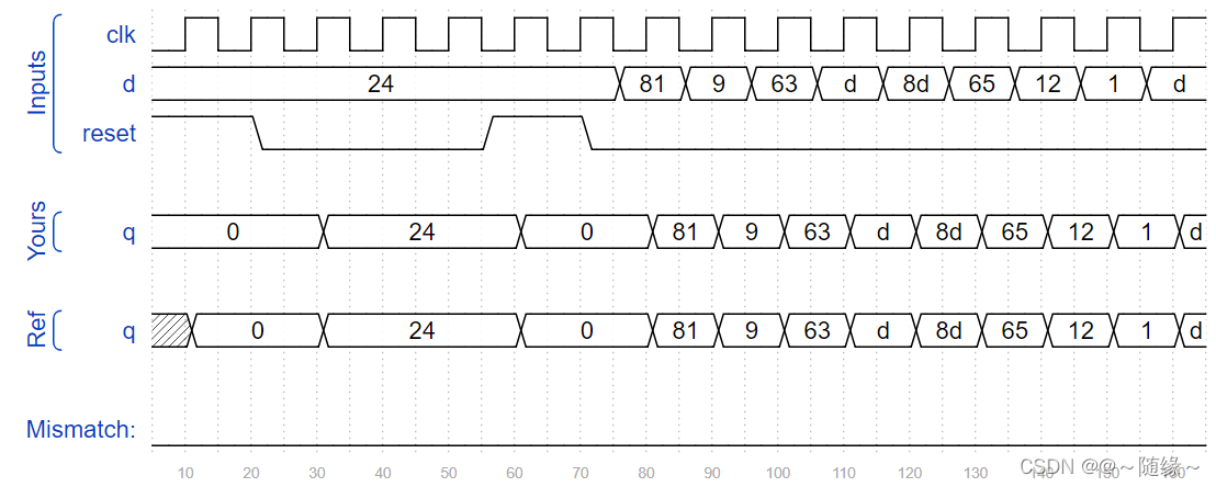
创建一个16D触发器,有时我们仅需要修改部分触发器中的值。字节使能信号控制当前时钟周期中16个寄存器中哪个字节需被修改。byteena[1]控制高字节d[15:8],而byteena[0]控制低字节d[7:0]。
resetn是一个同步,低复位信号。
所有的D触发器由时钟的上升沿触发。
module top_module (
    input clk,
    input resetn,
    input [1:0] byteena,
    input [15:0] d,
    output [15:0] q
);

    always @(posedge clk) begin
        if(resetn) begin
            if(byteena[1])
 最低0.47元/天 解锁文章


 1万+
1万+

 被折叠的 条评论
为什么被折叠?
被折叠的 条评论
为什么被折叠?
 到【灌水乐园】发言


