


 本文分享了使用Verilog进行卡诺图(Karnaugh Map)应用的四个实例,包括3-和4-变量逻辑电路设计,涉及SOP、POS形式的转换,以及最小项表达的实现。通过实际题目解析和解答,深入理解卡诺图化简技巧,并展示了如何将化简后的逻辑表达式转化为Verilog代码。
FPGA学习: Verilog刷题记录(9)
刷题网站 : HDLBits
第3章 : Circuits
第1大节 :Combinational Logic
第4小节 : Karnaugh Map to Circuit
- 3-variable
-
题目描述:Implement the circuit described by the Karnaugh map below.

-
题目分析:卡诺图的化简
-

-
解答:
/*我的解答*/ module top_module( input a, input b, input c, output out ); assign out = a | c | b; endmodule /*官网解答*/ module top_module( input a, input b, input c, output out ); // SOP form: Three prime implicants (1 term each), summed. // POS form: One prime implicant (of 3 terms) // In this particular case, the result is the same for both SOP and POS. assign out = (a | b | c); endmodule -
4-variable
-
题目描述:Implement the circuit described by the Karnaugh map below.

-
题目分析:这里选择圈0,然后最后结果整体取反

-
解答:
/*我的解答*/
module top_module(
    input a,
    input b,
    input c,
    input d,
    output out  );

    assign out = ~((a & b & ~c) | (b & ~c & d) | (a & c & ~d) | (~a & ~b & c & d));

endmodule

/*官网解答*/
无
-
-
4-variable
-
题目描述:Implement the circuit described by the Karnaugh map below.

-
题目分析:含有无关项的卡诺图化简,d可以根据需要为0或1,我的化简如下图
-

- 解答:
/*我的解答*/ module top_module( input a, input b, input c, input d, output out ); assign out = a | (~b & c); endmodule /*官网解答*/ 无 - 4-variable
-
题目描述:Implement the circuit described by the Karnaugh map below.

-
题目分析:这种形式,通常是异或的标志
-
解答:
/*我的解答*/
module top_module(
  input a,
  input b,
  input c,
  input d,
  output out  );

  assign out = a ^ b ^ c ^ d;

endmodule

/*官网解答*/
无
-
- Minimum SOP and POS
-
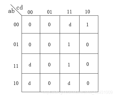
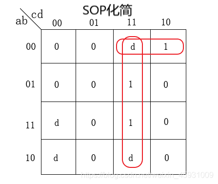
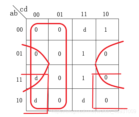
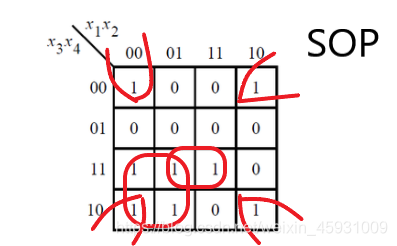
题目描述:A single-output digital system with four inputs (a,b,c,d) generates a logic-1 when 2, 7, or 15 appears on the inputs, and a logic-0 when 0, 1, 4, 5, 6, 9, 10, 13, or 14 appears. The input conditions for the numbers 3, 8, 11, and 12 never occur in this system. For example, 7 corresponds to a,b,c,d being set to 0,1,1,1, respectively.
Determine the output out_sop in minimum SOP form, and the output out_pos in minimum POS form.
-
题目分析:根据题目描述可以得到卡诺图如下,以及它的化简
- SOP form 即与或式,对应于卡诺图就是圈1即可
- POS form 即或与式, 对应于卡诺图就是圈0后,整体取反
-
解答:
/*我的解答*/
module top_module (
    input a,
    input b,
    input c,
    input d,
    output out_sop,
    output out_pos
);

    assign out_sop = (~a & ~b & c) | (c & d);
    assign out_pos = ~((~c) | (b & ~d) | (a & ~d));
endmodule

/*官网解答*/
无
-
- Karnaugh map
-
题目描述:Consider the function f shown in the Karnaugh map below.

-
题目分析:
![[外链图片转存失败,源站可能有防盗链机制,建议将图片保存下来直接上传(img-sseabEdo-1614062861621)(D:\Linux-windows\HDLBits\Karnagh\K6_a.png)]](https://i-blog.csdnimg.cn/blog_migrate/33684117589afc6257a493ec976d7c73.png#pic_center)
-
解答:
/*我的解答*/
module top_module (
    input [4:1] x,
    output f );

    assign f = (x[1] & x[2] & ~x[3] ) | (~x[1] & x[3]);

endmodule

/*官网解答*/
无
-
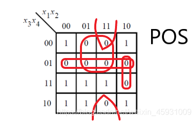
- Karnaguh map
-
题目描述:Consider the function f shown in the Karnaugh map below. Implement this function.
(The original exam question asked for simplified SOP and POS forms of the function.)
![[外链图片转存失败,源站可能有防盗链机制,建议将图片保存下来直接上传(img-5jnxjBSo-1614062861622)(https://hdlbits.01xz.net/mw/thumb.php?f=Exams_2012q1g.png&width=195)]](https://i-blog.csdnimg.cn/blog_migrate/519022012a3d283b263ce9fe08b3db17.png#pic_center)
-
题目分析:
-
解答:
/*我的解答*/
module top_module (
    input [4:1] x,
    output f
);

   assign f = (~x[2] & ~x[4]) | (~x[1] & x[3]) | (x[2] & x[3] & x[4]);
 //assign f = ~((x[2] & ~x[3]) | (~x[3] & x[4]) | (x[1] & ~x[2] & x[4] ) | (x[1] & x[2] & ~x[4]));

endmodule

/*官网解答*/
无
-
- K-map implemented with a multiplexer
-
题目描述:For the following Karnaugh map, give the circuit implementation using one 4-to-1 multiplexer and as many 2-to-1 multiplexers as required, but using as few as possible. You are not allowed to use any other logic gate and you must use a and b as the multiplexer selector inputs, as shown on the 4-to-1 multiplexer below.
You are implementing just the portion labelled top_module, such that the entire circuit (including the 4-to-1 mux) implements the K-map.


-
题目分析:题目要求我们在不使用逻辑门的情况下实现顶层模块,我们需要根据卡诺图来看,大概思路就是ab取值固定时,看cd如何变化,也就是把卡诺图当成4列来看
![[外链图片转存失败,源站可能有防盗链机制,建议将图片保存下来直接上传(img-stNld4Qs-1614062861629)(D:\Linux-windows\HDLBits\Karnagh\K8.png)]](https://i-blog.csdnimg.cn/blog_migrate/250ea232f151744896cc9c71af49d805.png#pic_center)
- 红色那列对应mux_in[0],cd都为0的时候结果才为mux_in[0]=0,也就是或的关系
- 黄色那列对应mux_in[1], cd无论取什么值,都为0 mux_in[1]=0
- 蓝色那列对应mux_in[2], cd都为0时,或c=1,d=0时,也就是**~d**时结果为1 mux_in[3]=1
- 绿色那列对应mux_in[3], cd都为1时,结果为1 mux_in[3] = 1
- 因为题目要求不用逻辑门,我们可以用三目运算符来表述
-
解答:
/*我的解答*/
module top_module (
    input c,
    input d,
    output [3:0] mux_in
);

    assign mux_in[0] = c ? 1 :(d ? 1 : 0);  //这就表示说cd全为假时,结果才为0
    assign mux_in[1] = 1'b0 ; 			    //恒为0
    assign mux_in[2] = d ? 0 : 1            //这表示说~d时,结果才为1
    assign mux_in[3] = c ? (d ? 1 : 0) : 0;//cd都为真时,取值为1

endmodule
/*官网解答*/
module top_module (
	input c,
	input d,
	output [3:0] mux_in
);

	// After knowing how to split the truth table into four columns,
	// the rest of this question involves implementing logic functions
	// using only multiplexers (no other gates).
	// I will use the conditional operator for each 2-to-1 mux: (s ? a : b)
	assign mux_in[0] = (c ? 1 : (d ? 1 : 0));	// 2 muxes: c|d
	assign mux_in[1] = 0;						// No muxes:  0
	assign mux_in[2] = d ? 0 : 1;				// 1 mux:    ~d
	assign mux_in[3] = c ? (d ? 1 : 0) : 0;		// 2 muxes: c&d

endmodule
-
总结
-
卡诺图化简
1. SOP form 即与或式,对应于卡诺图就是圈1即可
2. POS form 即或与式, 对应于卡诺图就是圈0后,整体取反


 771
771

 被折叠的 条评论
为什么被折叠?
被折叠的 条评论
为什么被折叠?
 到【灌水乐园】发言


