


FPGA教程系列-Vivado中读取ROM中数据
- 生成coe文件教程
https://blog.youkuaiyun.com/ccsss22/article/details/124441036
本实验主要读取rom中的数据。rom中存储的数据为coe文件,用matlab可以生成。
生成coe文件
clc;
clear;
close all;
warning off;
addpath(genpath(pwd));
% --- 1. Parameters ---
num_points = 512;         % Number of points in the sine wave (e.g., 256 for a 256-depth ROM)
amplitude_scale = 1023;   % Scaling factor to match the desired integer range.
                          % 1023 corresponds to a 10-bit unsigned range (0-1023) or
                          % an 11-bit signed range centered at 0 (-1023 to 1023).
                          % We will generate a signed sine wave.
% --- 2. Generate the Sine Wave ---
% Create a time vector from 0 to 2*pi for one full cycle
t = linspace(0, 2*pi, num_points);
% Generate the floating-point sine wave
y_continuous = sin(t);
% Quantize and scale the wave to integer values
% The result will be in the range [-1023, 1023]
y_quantized = round(amplitude_scale * y_continuous);
% --- 3. Write to .coe File ---
file_name = 'sine_wave.coe';
fid = fopen(file_name, 'w');
% Check if the file opened successfully
if fid == -1
    error('Could not open file for writing.');
end
% Write the .coe file header
fprintf(fid, 'memory_initialization_radix=10;\n');
fprintf(fid, 'memory_initialization_vector =\n');
% Write the data vector
for i = 1:length(y_quantized)
    fprintf(fid, '%d', y_quantized(i));
    % Add a comma after each value except the last one
    if i < length(y_quantized)
        fprintf(fid, ',\n');
    else
        fprintf(fid, ';'); % End the vector with a semicolon
    end
end
% Close the file
fclose(fid);
fprintf('Successfully generated %s with %d data points.\n', file_name, num_points);
% --- 4. Plot the Generated Wave for Verification ---
figure;
plot(y_quantized);
title('Generated Quantized Sine Wave');
xlabel('Sample Index');
ylabel('Amplitude (Integer Value)');
grid on;
axis tight; % Fit the axes tightly to the data
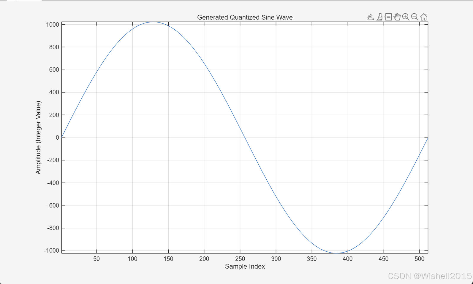
用上述程序,生成一个sine_wave.coe文件,生成的波形如图:
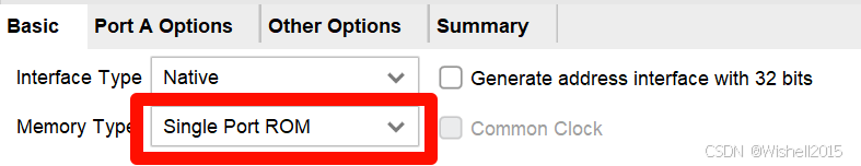
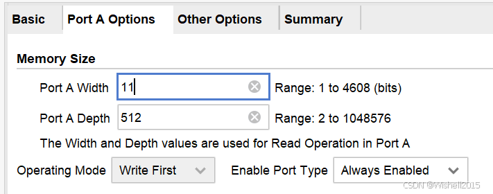
生成IP核
本仿真采用ROM核,位数11位,深度512.
编写top文件
`timescale 1ns / 1ps

module rom_top(
input clka,
input rsta,
output signed[10:0] douta
    );

reg[8:0] addra;
always @(posedge clka or posedge rsta)
begin
     if(rsta)
     begin
     addra <= 9'd0;
     end
else begin
          if(addra == 9'd511)
          addra <= 9'd0;
          else
          addra <= addra+ 9'd1;
     end
end


blk_mem_gen_0 blk_mem_gen_u (
  .clka(clka),            // input wire clka
  .rsta(rsta),            // input wire rsta
  .addra(addra),          // input wire [8 : 0] addra
  .douta(douta),          // output wire [10 : 0] douta
  .rsta_busy()  // output wire rsta_busy
);

endmodule
编写Testbench
`timescale 1ns / 1ps

module rom_top_tb;
reg clka;
reg rsta;
wire signed[10:0]douta;
rom_top rom_top_u(
.clka  (clka),
.rsta  (rsta),
.douta (douta)
);
initial
begin
clka = 1'b1;
rsta = 1'b1;
#100
rsta = 1'b0;
end
always #5 clka = ~clka;
endmodule
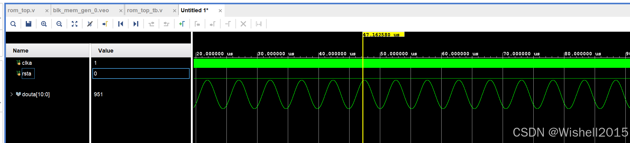
仿真分析
最终输出的结果,就是读取coe文件中的波形,即sin函数。当然可以用matlab生成各种各样的波形来进行读取。
工程文件:https://download.youkuaiyun.com/download/fantasygwh2015/92292030


 673
673

 被折叠的 条评论
为什么被折叠?
被折叠的 条评论
为什么被折叠?
 到【灌水乐园】发言


