


 本文详细介绍了使用Flash的页编程指令PP进行编程的过程,涉及擦除操作、SPI模块的状态机设计以及相应的控制信号编码,展示了如何通过状态机来控制SPI传输数据和执行指令的过程。
本实验重点学习了:
flash的页编程指令pp。
在写之前要先进行擦除(全擦除和页擦除);
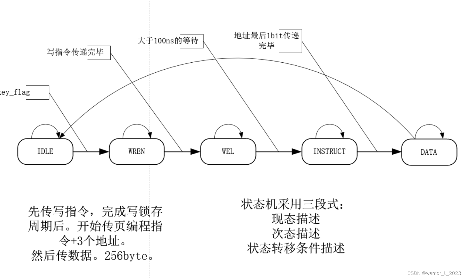
本实验:先传写指令,然后进入写锁存周期,然后传页编程指令,+3个地址;
然后传数据,奇数传55,偶数传aa。
在之前扇区擦除的代码上改改就行了。加一个功能就是传入数据大于256个时候,mosi一直拉高。
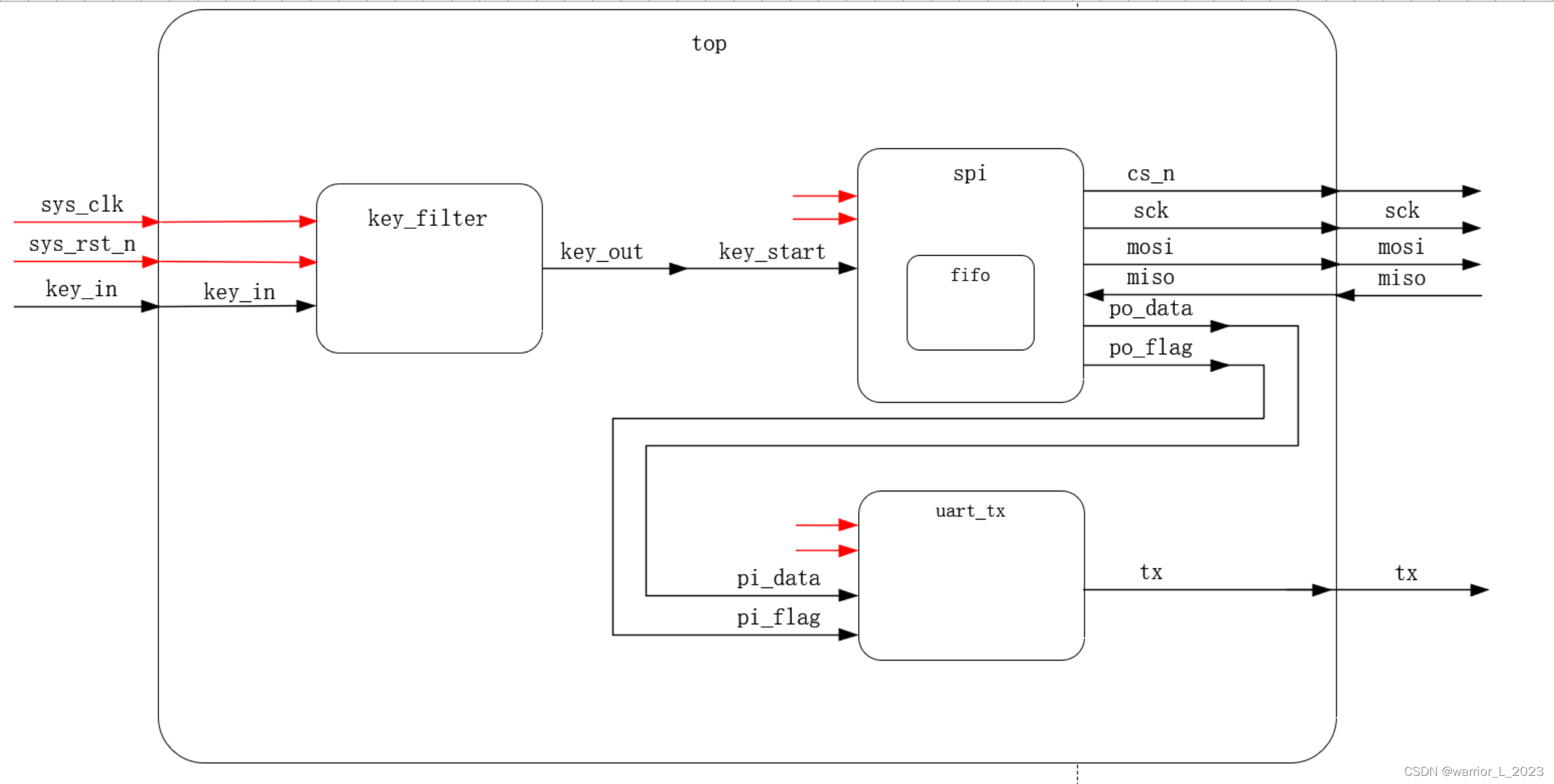
模块框图:
状态机:
代码:
只放spi模块的。因为其他代码和扇区擦除指令是一样的。
module spi (
input wire sys_clk ,
input wire sys_rst_n ,
input wire key_start ,
output wire miso ,
output reg mosi ,
output reg cs_n ,
output reg sck
);
// parameter
parameter COMD_W = 8'h06 , // 写指令, 先发送写指令,进入写锁存周期
COMD_P = 8'h02 , // 页写指令
MAX_NUM = 32'd270 ; // 要发送指令+地址+数据的字节数。 2 + 3 + 100
parameter ADR_SE = 8'h00 , // 扇区地址 adress secter
ADR_PA = 8'h04 , // 页地址 adress page
ADR_BY = 8'h00 ; // 字节地址 adress byte
parameter DATA_ODD = 8'h55 , // odd 奇数
DATA_EVE = 8'haa ; // even 偶数
parameter IDLE = 5'b00001 ,
WREN = 5'b00010 ,
WEL = 5'b00100 ,
INST = 5'b01000 , // instruct 传送pp指令和addr
DATA = 5'b10000 ; // instruct 传送要写入的数据。
// wire signal degine
wire IDLEtoWREN;
wire WRENtoWEL ;
wire WRENtoINST;
wire INSTtoDATA;
wire DATAtoIDLE;
// reg signal define
reg [19:0] data_num ; // 记录传递的数据,如果超过256个,那么mosi将会一直拉高(传1).
reg [4:0] state_c ;
reg [4:0] state_n ;
reg [3:0] cnt_20ns ;
reg [3:0] cnt_bit ;
reg [31:0] cnt_byte ;
reg flag_bit ;
reg f_b_reg ; // flag_bit_reg的缩写
/****************************************************************************/
// 三段式状态机
// 现态与次态描述
// state_c
always @(posedge sys_clk or negedge sys_rst_n) begin
if(~sys_rst_n)
state_c <= IDLE ;
else
state_c <= state_n ;
end
// state_n
always @(*) begin
case (state_c)
IDLE :if(IDLEtoWREN)
state_n <= WREN ;
else
state_n <= IDLE ;
WREN :if(WRENtoWEL)
state_n <= WEL ;
else
state_n <= WREN ;
WEL :if(WRENtoINST)
state_n <= INST ;
else
state_n <= WEL ;
INST :if(INSTtoDATA)
state_n <= DATA ;
else
state_n <= INST ;
DATA :if(DATAtoIDLE)
state_n <= IDLE ;
else
state_n <= DATA ;
default: state_n <= IDLE ;
endcase
end
// 状态转移描述
assign IDLEtoWREN = ( state_c == IDLE) && ( key_start ) ;
assign WRENtoWEL = ( state_c == WREN) && ( f_b_reg ) ;
assign WRENtoINST = ( state_c == WEL ) && ( cnt_20ns == 6 ) ;
assign INSTtoDATA = ( state_c == INST) && ( f_b_reg ) ;
assign DATAtoIDLE = ( state_c == DATA) && ( f_b_reg && cnt_byte != 5) ; // 至少传递一个数据。否则会卡死在这个状态。
// 相关信号描述
// reg [3:0] cnt_20ns ;
always @(posedge sys_clk or negedge sys_rst_n) begin
if(~sys_rst_n)
cnt_20ns <= 4'd0 ;
else
case (state_c)
IDLE : cnt_20ns <= 4'd0 ;
WREN : if(cnt_20ns || f_b_reg)
cnt_20ns <= 4'd0 ;
else
cnt_20ns <= cnt_20ns + 1'b1 ;
WEL : if(cnt_20ns == 6) // 60x20ns==120ns
cnt_20ns <= 4'd0 ;
else
cnt_20ns <= cnt_20ns + 1'b1 ;
INST : if(cnt_20ns) // 由于下一个状态是发送数据,sck和cnt_20_ns的变换规律与INST相同。所以不需要f_b_reg。
cnt_20ns <= 4'd0 ;
else
cnt_20ns <= cnt_20ns + 1'b1 ;
DATA : if(cnt_20ns || (f_b_reg && cnt_byte != 5))
cnt_20ns <= 4'd0 ;
else
cnt_20ns <= cnt_20ns + 1'b1 ;
default: cnt_20ns <= 4'd0 ;
endcase
end
// reg [3:0] cnt_bit ;
always @(posedge sys_clk or negedge sys_rst_n) begin
if(~sys_rst_n)
cnt_bit <= 4'd0 ;
else
case (state_c)
IDLE : cnt_bit <= 4'd0 ;
WREN : if(!cnt_20ns && sck && cnt_bit == 7)
cnt_bit <= 4'd0 ;
else if(!cnt_20ns && sck)
cnt_bit <= cnt_bit + 1'b1 ;
WEL : cnt_bit <= 4'd0 ;
INST : if(!cnt_20ns && sck && cnt_bit == 7)
cnt_bit <= 4'd0 ;
else if(!cnt_20ns && sck)
cnt_bit <= cnt_bit + 1'b1 ;
DATA : if(!cnt_20ns && sck && cnt_bit == 7)
cnt_bit <= 4'd0 ;
else if(!cnt_20ns && sck)
cnt_bit <= cnt_bit + 1'b1 ;
default: cnt_bit <= 4'd0 ;
endcase
end
// reg [31:0] cnt_byte
always @(posedge sys_clk or negedge sys_rst_n) begin
if(~sys_rst_n)
cnt_byte <= 32'd0 ;
else if(cnt_bit == 7 && !cnt_20ns && sck && cnt_byte == MAX_NUM - 1) // 计数到传送字节的最大值。
cnt_byte <= 32'd0 ;
else if(cnt_bit == 7 && !cnt_20ns && sck)
cnt_byte <= cnt_byte + 1'b1 ;
else
cnt_byte <= cnt_byte ;
end
// reg flag_bit ;
always @(posedge sys_clk or negedge sys_rst_n) begin
if(~sys_rst_n)
flag_bit <= 1'b0 ;
else
case (state_c)
IDLE : flag_bit <= 1'b0 ;
WREN : if(cnt_bit == 7 && sck && !cnt_20ns)
flag_bit <= 1'b1 ;
else
flag_bit <= flag_bit ;
WEL : flag_bit <= 1'b0 ;
INST : if(cnt_bit == 7 && sck && !cnt_20ns && cnt_byte == 4)
flag_bit <= 1'b1 ;
else
flag_bit <= flag_bit ;
DATA : if(cnt_bit == 0 && cnt_byte == 5)
flag_bit <= 1'b0 ;
else if(cnt_bit == 7 && sck && !cnt_20ns && cnt_byte == MAX_NUM - 1)
flag_bit <= 1'b1 ;
else
flag_bit <= flag_bit ;
default: flag_bit <= 1'b0 ;
endcase
end
// reg f_b_reg ;
always @(posedge sys_clk or negedge sys_rst_n) begin
if(~sys_rst_n) begin
f_b_reg <= 1'b0 ;
end else begin
f_b_reg <= flag_bit ;
end
end
// reg [19:0] data_num
always @(posedge sys_clk or negedge sys_rst_n) begin
if(~sys_rst_n)
data_num <= 20'd0 ;
else if(state_c == DATA && cnt_bit == 7 && !cnt_20ns && sck)
data_num <= data_num + 1'b1 ;
else if(state_c != DATA)
data_num <= 20'd0 ;
else
data_num <= data_num ;
end
// output signal
// wire miso ,
assign miso = 1'bz ;
// mosi
always @(posedge sys_clk or negedge sys_rst_n) begin
if(~sys_rst_n)
mosi <= 1'b0 ;
else
case (state_c)
IDLE : mosi <= 1'b0 ;
WREN : if(!cnt_bit) // (cnt_bit == 0)
mosi <= COMD_W[7] ;
else if(cnt_20ns && sck)
mosi <= COMD_W[7 - cnt_bit] ;
else
mosi <= mosi ;
WEL : mosi <= 1'b0 ;
INST : case (cnt_byte)
1:
begin
if(!cnt_bit)
mosi <= COMD_P[7] ;
else if(cnt_20ns && sck)
mosi <= COMD_P[7 - cnt_bit] ;
else
mosi <= mosi ;
end
2:
begin
if(!cnt_bit)
mosi <= ADR_SE[7] ;
else if(cnt_20ns && sck)
mosi <= ADR_SE[7 - cnt_bit] ;
else
mosi <= mosi ;
end
3:
begin
if(!cnt_bit)
mosi <= ADR_PA[7] ;
else if(cnt_20ns && sck)
mosi <= ADR_PA[7 - cnt_bit] ;
else
mosi <= mosi ;
end
4:
begin
if(!cnt_bit)
mosi <= ADR_BY[7] ;
else if(cnt_20ns && sck)
mosi <= ADR_BY[7 - cnt_bit] ;
else
mosi <= mosi ;
end
5:
begin
if(!cnt_bit) // 由于当cnt_byte == 5 时,有一段state_c没有立即跳转到data状态。
mosi <= DATA_ODD[7] ;
else if(cnt_20ns && sck)
mosi <= DATA_ODD[7 - cnt_bit] ;
else
mosi <= mosi ;
end
default: mosi <= 1'b0 ;
endcase
DATA : if(data_num <= 255) begin
if(cnt_byte[0]) begin // 二进制最低为奇偶标志位,1表示奇位,发送数据5。
if(!cnt_bit)
mosi <= DATA_ODD[7] ;
else if(cnt_20ns && sck)
mosi <= DATA_ODD[7 - cnt_bit] ;
else
mosi <= mosi ;
end else begin // cnt_byte[0] == 0 偶数。发送数据a
if(!cnt_bit)
mosi <= DATA_EVE[7] ;
else if(cnt_20ns && sck)
mosi <= DATA_EVE[7 - cnt_bit] ;
else
mosi <= mosi ;
end
end else begin
mosi <= 1'b1 ; // 大于256个数据之后,mosi就一直传递1.
end
default: mosi <= 1'b0 ;
endcase
end
// reg cs_n ,
always @(posedge sys_clk or negedge sys_rst_n) begin
if(~sys_rst_n) begin
cs_n <= 1'b1 ;
end else begin
case (state_c)
IDLE : if(key_start)
cs_n <= 1'b0 ;
else
cs_n <= 1'b1 ;
WREN : if(f_b_reg)
cs_n <= 1'b1 ;
else
cs_n <= cs_n ;
WEL : if(cnt_20ns == 6)
cs_n <= 1'b0 ;
else
cs_n <= cs_n ;
INST : cs_n <= 1'b0 ;
DATA : if(f_b_reg && cnt_byte != 5 )
cs_n <= 1'b1 ;
else
cs_n <= cs_n ;
default: cs_n <= 1'b1 ;
endcase
end
end
// reg sck
always @(posedge sys_clk or negedge sys_rst_n) begin
if(~sys_rst_n)
sck <= 1'b0 ;
else
case (state_c)
IDLE : sck <= 1'b0 ;
WREN : if(cnt_20ns)
sck <= ~sck ;
else
sck <= sck ;
WEL : sck <= 1'b0 ;
INST : if(cnt_20ns)
sck <= ~sck ;
else
sck <= sck ;
DATA : if(cnt_20ns)
sck <= ~sck ;
else
sck <= sck ;
default: sck <= 1'b0 ;
endcase
end
endmodule
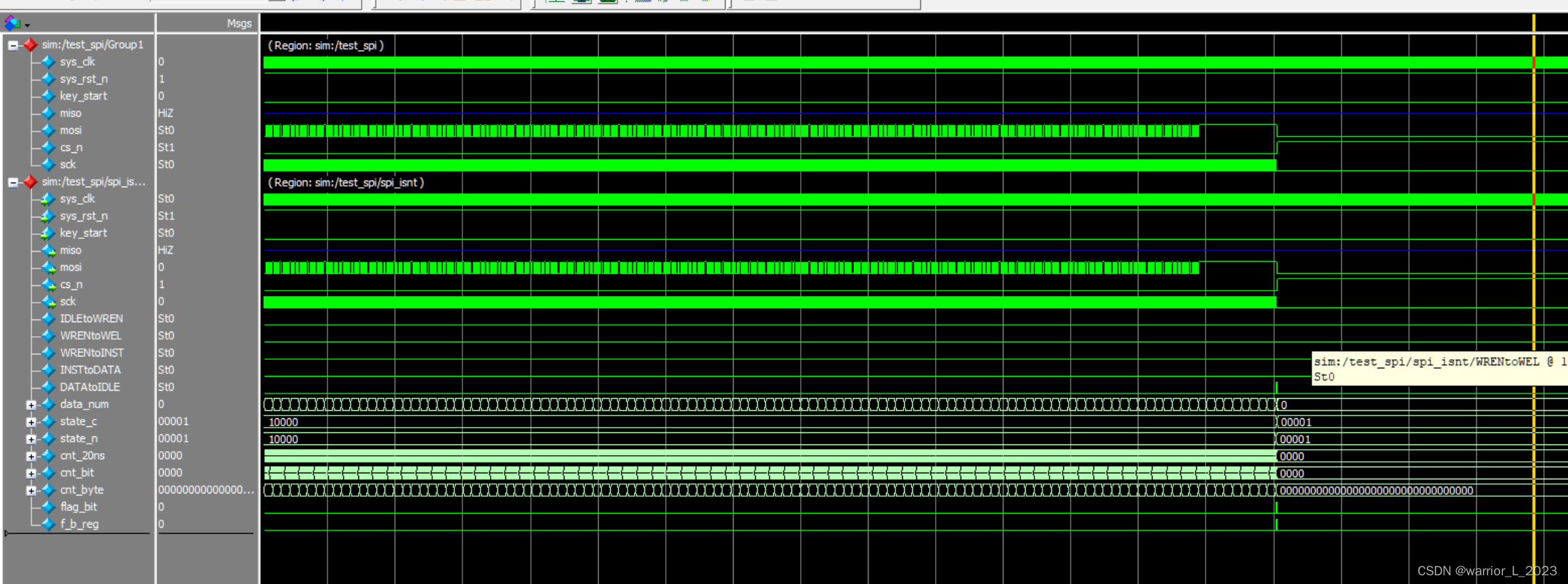
仿真波形:


 5794
5794

 被折叠的 条评论
为什么被折叠?
被折叠的 条评论
为什么被折叠?
 到【灌水乐园】发言


