


一、特性
1、SMBus, Two-Wire, and I2C Interface
Register bytes are sent with the most significant byte first, followed by the least significant byte
2、Supply Range: 1.4 to 3.6 V
3、工作温度:-40~125
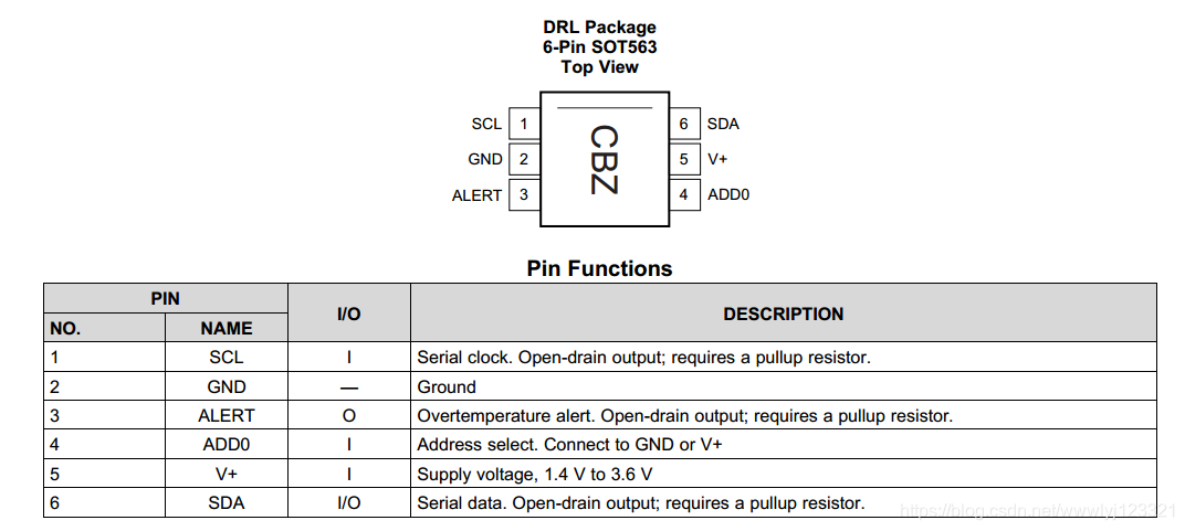
4、引脚说明
ALERT用于温度阈值时报警、ADD0用于地址选择。
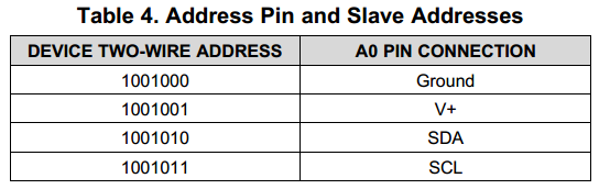
TMP102可以设置四个地址,对应着分别接到-、+、SDA、SCL,如下图所示:
二、几种工作模式
1、Continuos-Conversion Mode(默认)
每隔一段时间自动转换,转换结果自动保存在temperature register,转换频率通过配置寄存器中的CR1 and CR0设置。
2、Extended Mode (EM)
In Normal mode, the Temperature Register and high- and low-limit registers use a 12-bit data format,这种模式是为了兼容TMP75传感器。
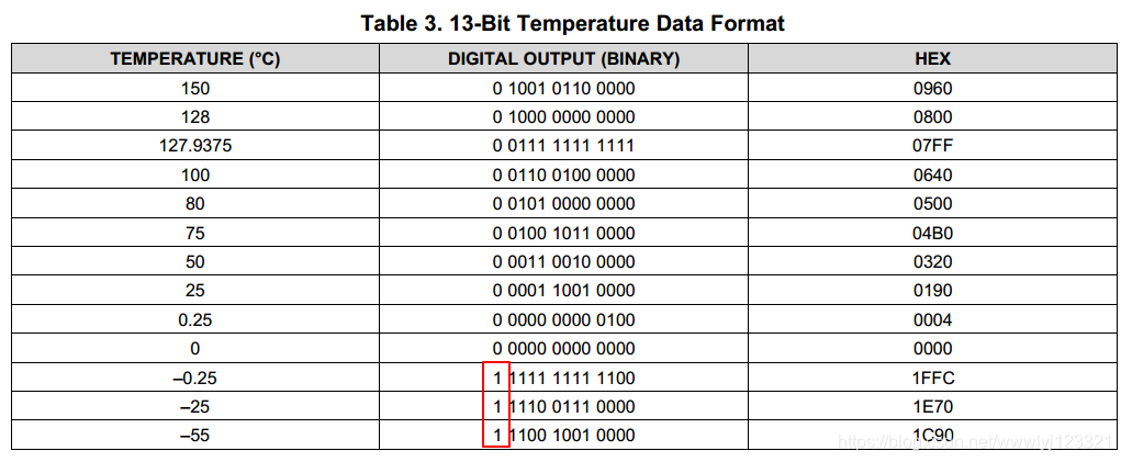
Extended mode (EM = 1) ,数据格式是13bit,这种模式allows measurement of temperatures above 128°C 。
3、Shutdown Mode (SD)
这种模式是最省电的,进入这种模式下通常电流小于0.5ua。可以通过读写配置寄存器的SD位来强制进入该模式或者获取目前的工作状态。当读SD位是零,表示正在进行ad转换,当读到是1表示转换完成,进入SD模式。
4、One-Shot/Conversion Ready (OS)
单次触发模式。可以通过写配置寄存器的OS位触发一次AD转换,从而可以更加灵活的实现转换频率。
5、Thermostat Mode (TM)
Comparator Mode (TM = 0)
Interrupt Mode (TM = 1)
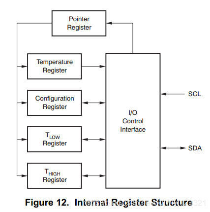
三、内部寄存器
TMP102内部总共有五个寄存器:Pointer Register(指针寄存器)、Temperature Register(温度寄存器)、Configuration Register(配置寄存器)、T LOW Register(低温阈值寄存器)、T HIGH Register(高温阈值寄存器)。
1、五个寄存器的逻辑关系
IIC读写控制默认就是指向指针寄存器,而这个指针会根据数值不同而指向不同的寄存器。
比如往TMP102芯片里写0x01时,它会直接对应到配置寄存器Configuration Register,再根据后面的读、写标志位,来判断是对Configuration Register读还是写。
2、各个寄存器的详细阐述
a)Pointer Register(指针寄存器)
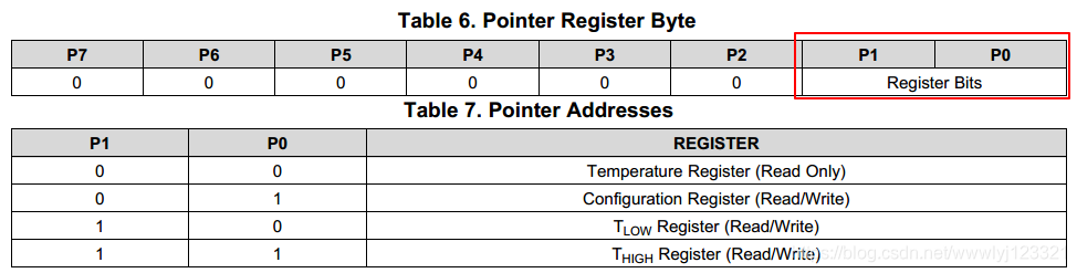
通过低两位指定接下来要控制哪个寄存器,上电初始值是0,也就是读温度寄存器
b)Temperature Register(温度寄存器)
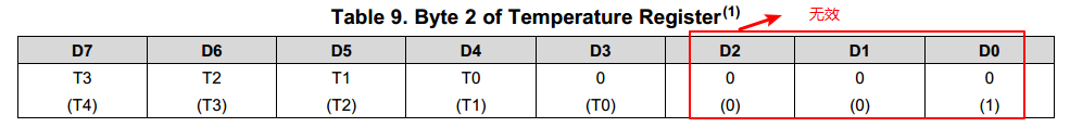
温度寄存器总共有两个字节(Byte1是MSB Byte2是LSB),保存了12位或13位的温度数据(normal mode (EM bit = 0) or extended mode (EM bit = 1),分别对应12位精度与13位精度),其中Byte2的低3位无用。
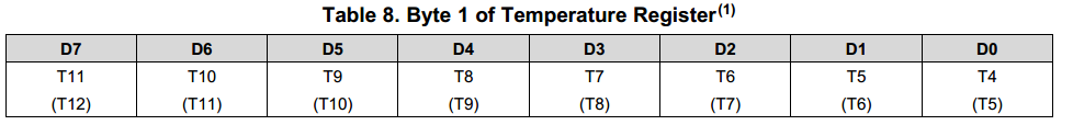
在12bit模式下,bit T11表示温度的正负;在13bit模式下,bit T12表示温度的正负。
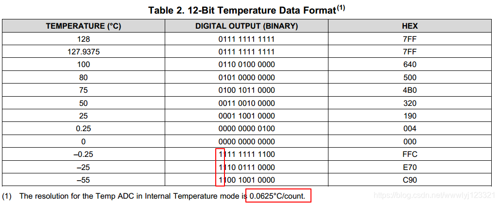
12bit正温度举例:
Example: 0011 0010 0000 = 320h = 800 × (0.0625°C / LSB) = 50°C
12bit负温度举例:
Example: 1110 0111 0000
先转换成为补码:0001 1000 1111
在补码的基础上加1:0001 1000 1111+1 = 0001 1001 0000 = 190h = 400; 400 × (0.0625°C / LSB) = 25°C = (|–25°C|);
(|–25°C|) × (–1) = –25°C
c)Configuration Register(配置寄存器)
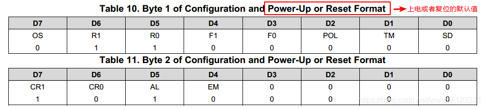
OS(One-Shot):当在shutdown模式下,向该位写1启动一次温度转换。转换完成后,又进入shutdown模式
When the device is in Shutdown Mode, writing a 1 to the OS bit starts a single temperature conversion. During the conversion, the OS bit reads '0'. The device returns to the shutdown state at the completion of the single conversion.
R1/R0:转换器分辨率位(R1 and R0, are read-only bits),上电默认0x11,表示12位分辨率。
F1/F0:当温度超出用户设置的上限或者下限的连续n次时候,才触发alert引脚。这个功能是为了降低环境噪声引起的误报。

POL:设置Alert Pin的输出极性。如下图所示
If the POL bit is set to 0 (default),the ALERT pin becomes active low. When the POL bit is set to 1, the ALERT pin becomes active high and the state of the ALERT pin is inverted.
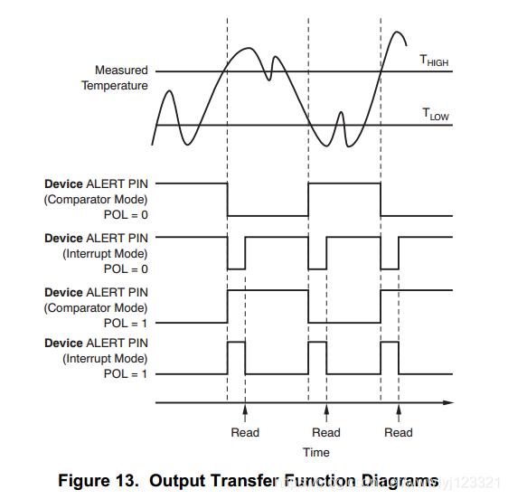
TM:“0”表示比较模式;“1”表示中断模式。从上图也可以看出,其实两种模式其实就是Alert输出电平信号的差异,一种是跳变,一种是持续。
SD:关断模式(Shutdown mode),“0”表示维持数据转换(ADC)状态,“1”表示现有数据转换完成,进入关断模式。强制进入关断模式能降低功耗。
Byte2的各位数含义:
CR1/CR0(Conversion Rate):设置在continuos conversion mode(默认模式)下的数据转换速率。每一次转换完成会将转换结果存放在temperature register。

AL(Alert):read-only。
Reading the AL bit provides information about the comparator mode status.The state of the POL bit inverts the polarity of data returned from the AL bit. When the POL bit equals 0, the AL bit reads as 1 until the temperature equals or exceeds T(HIGH) for the programmed number of consecutive faults, causing the AL bit to read as 0. The AL bit continues to read as 0 until the temperature falls below T(LOW) for the programmed number of consecutive faults, when it again reads as 1. The status of the TM bit does not affect the status of the AL bit
EM(Extended-Mode):“0”表示正常工作模式,数据格式12位;“1”表示扩展工作模式,数据格式13位。
d)T LOW Register(低温阈值寄存器)
设置最低温度阈值的
e)T HIGH Register(高温阈值寄存器)
设置最高温度阈值
四、使用实例
To communicate with the TMP102, the master must first address slave devices via a slave address byte. The slave address byte consists of seven address bits, and a direction bit indicating the intent of executing a read or write operation.
host写TMP102:
1、host发送slave address(with the R/W bit Low)
2、Host向TMP102写pointer register,也就是确定了接下来要真正操作哪个寄存器
3、Host向TMP102写一个字节或者多个字节到pointer register指向的寄存器
4、host发送START or STOP
Slave Receiver Mode
The first byte transmitted by the master is the slave address, with the R/W bit low. The TMP102 then acknowledges reception of a valid address. The next byte transmitted by the master is the pointer register. The TMP102 then acknowledges reception of the pointer register byte. The next byte or bytes are written to the register addressed by the pointer register. The TMP102 acknowledges reception of each data byte. The master can terminate data transfer by generating a START or STOP condition..
host读TMP102:
1、host发送slave address(with the R/W bit high)
2、TMP102向host发送当前pointer register指向的寄存器的内容的MSB
3、TMP102向host发送当前pointer register指向的寄存器的内容的LSB
4、host发送Noack或者START or STOP
Slave Transmitter Mode
The first byte transmitted by the master is the slave address, with the R/W bit high. The slave acknowledges reception of a valid slave address. The next byte is transmitted by the slave and is the most significant byte of the register indicated by the pointer register. The master acknowledges reception of the data byte. The next byte transmitted by the slave is the least significant byte. The master acknowledges reception of the data byte. The master terminates data transfer by generating a Not-Acknowledge on reception of any data byte, or generating a START or STOP condition.
ti官方提供的arduino部分代码:
      temp[0] = Wire.read();
      temp[1] = Wire.read();

      //ignore the lower 4 bits of byte 2
      temp[1] = temp[1] >> 4;
      //combine to make one 12 bit binary number
      tempc = ((temp[0] << 4) | temp[1]);

      //Convert to celcius (0.0625C resolution) and return
      return tempc*0.0625;
ref:
https://blog.youkuaiyun.com/feilusia/article/details/50610600
https://www.ti.com/lit/ds/symlink/tmp102.pdf
https://www.ti.com.cn/product/cn/TMP102#design-development##software-development


 607
607

 被折叠的 条评论
为什么被折叠?
被折叠的 条评论
为什么被折叠?
 到【灌水乐园】发言


