


1 PrimeTime基础
1.1 启动primeTime
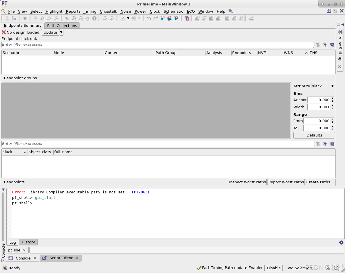
图形化界面:primetime
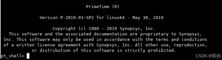
命令行启动:pt_shell
1.2 PrimeTime环境
set search_path [list <path>]
set link_path [list {*} fast.db typical.db slow.db]
1.3 读入设计
read_db <path>/<design_name>.db
read_verilog <path>/<design_name>.v
read_vhdl <path>/<design_name>.vhd
read_edif <path>/<design_name>.edf
1.4 设计约束、负载和时序约束
与DC综合时进行的时钟约束相同。
1.5 时序分析命令
set_disable_timing
report_disable_timing
set_input_transition
report_case_analysis
report_timing
report_constraint
report_bottleneck
2 静态时序分析
2.1 分析内容
通常,对设计进行如下4种类型的分析:
(1)从原始输入到设计中所有触发器;
(2)从触发器到触发器;
(3)从触发器到设计的原始输出;
(4)从设计的原始输入到原始输出;
所有这4种分析都能用如下命令来完成:
report_timing -from [all_inputs] -to [all_registers -data_pins]
report_timing -from [all_registers -clock_pins] -to [all_registers -data_pins]
report_timing -from [all_registers -clock_pins] -to [all_outputs]
report_timing -from [all_inputs] -to [all_outputs]
也可以采用如下命令:
report_timing -to [all_registers -data_pins]
report_timing  -to [all_outputs]
2.2 时序例外
2.2.1 多周期路径
set_multicycle_path <multiplier value> -from <from list> -to <to list>
2.2.2 伪路径
set_false_path -from <module/port> -to <module/port>
2.3 布线前建立时间STA的PT脚本
#Define the design and read the netlist only
set active_design <design name>
read_db -netlist_only $active_design.db
# or use the following command to read the Verilog netlist.
# read_verilog $active_design.v
current_design $active_design

set_wire_load_model <wire-load model name>
set_wire_load_mode <top |enclosed |segmented>

set_operating_conditions <worst-case operating conditions>

#Assuming the 50pf load requirement for all outputs
set_load 50.0 [all _outputs]
# Assuming the clock name is CLK with a period of 30ns.
# The latency and transition are frozen to approximate the post-routed values.
create_clock -period 30 -waveform [0 15] CLK
set_clock_latency 3.0 [get_clocks CLK]
set_clock_transition 0.2 [get_clocks CLK]
set_clock_uncertainty 1.5 -setup [get_clocks CLK]
# The input and output delay constraint values are assumed
# to be derived from the design specifications.
set_input_delay 15.0 -clock CLK [all_inputs]
set_output_delay 10.0 -clock CLK [all_outputs]

set TESTMODE [getenv TESTMODE]
if {$TESTMODE == 1} {
	set_case_analysis 1 [get_port bist_mode]
}else {
	set_case_analysis 0 [get_port bist_mode]
}
# The following command determines the overall health of the design.
report_constraint -all_violators
# Extensive analysis is performed using the following commands.
report_timing -to [all_registers -data_pins]
report_timing -to [all_outputs]
2.4 TCL脚本
# primetime tcl

# ###############################
#   set library   #
# ###############################
set search_path {./lib}
set link_path {your_library.db}


# ###############################
#   read design   #
# ###############################
read_verilog ./output/top_scan.vg

link_design top

list_designs
report_cell > ./pt/report_cell.txt


# ###############################
#   set load   #
# ###############################
set_wire_load_mode top
# set_wire_load_model -name large_wl
set_wire_load_mode segmented
list_libraries
# report_lib slow

# ###############################
#   define IO port name   #
# ###############################
set clk [get_clocks clk]
set rst_n [get_ports rst_n]
set general_inputs [list A B C test_si test_se]
set outputs [list X Y Z]

# ###############################
#   set constraints   #
# ###############################
create_clock -period 10 [get_ports clk]
set_clock_uncertainty 0.5 $clk
set_clock_latency -min 3.5 $clk
set_clock_latency -max 5.5 $clk
set_clock_transition -min 0.25 $clk
set_clock_transition -max 0.3 $clk

set_max_fanout 4 [get_ports clk]
set_max_fanout 4 [get_ports $general_inputs]
set_input_delay -max 8 -clock clk [get_ports $general_inputs]
set_output_delay -max 8 -clock clk [get_ports $outputs]

set_max_area 0.0
check_timing

# ###############################
#   output   #
# ###############################

report_constraint -all_violators
report_constraint > ./pt/report_constraint.txt
# report_reference > ./pt/report_reference.txt
report_design > ./pt/report_design.txt
report_timing
write_script -format ptsh -output ./pt/top_scan.pt
# write_sdf -version 2.1 ./pt/top_scan.sdf

# ###############################
#   set exceptions   #
# ###############################
# set_false_path -from U3/OUTPUT_reg/CP -to U2/OUTPUT_reg/D
# set_multicycle_path -setup 2 -from INSTRUCTION -to U2/OUTPUT_reg
# update_timing
# report_exceptions
# report_exceptions -ignored
# report_constraint –all_violators
# report_timing
参考文章:
1、《高级ASIC芯片综合 使用Synopsys Design Compiler、Physical Compiler和PrimeTime》
2、https://blog.youkuaiyun.com/Anton_wzd/article/details/135574207
3、https://blog.youkuaiyun.com/qq_21842097/article/details/120261190
5、https://blog.youkuaiyun.com/ciscomonkey/article/details/126803541
6、https://blog.youkuaiyun.com/weixin_33597080/article/details/143337600


 356
356

 被折叠的 条评论
为什么被折叠?
被折叠的 条评论
为什么被折叠?
 到【灌水乐园】发言


