STA概念:一文了解NLDM与CCS

本文介绍了静态时序分析(STA)中的两种cell延迟模型——NLDM(非线性延迟模型)和CCS(复合电流源模型)。NLDM包括driver和receiver模型,但在小尺寸工艺中面临电阻和Miller效应问题。相比之下,CCS模型解决了这些问题,提供更精确的延迟和电流波形描述,尤其是在处理大电阻net和Miller效应时表现优越。

对于cell的delay的计算,由于规模的原因,是不可能通过晶体管级仿真进行的。

所以引入了静态时序分析的概念。

而在静态时序分析中,cell delay,是通过查找表并进行插值来得到的,从而大大减少了计算量,提高了工具的运行速度。

对cell delay的表征(characterization),有两种形式。

CCS:composite current source

NLDM:non linear delay model

CCS,已经被引用多年。目前,与nldm一样,已经成为了单元库的标配。

本文将简单介绍一下两种delay model,以及他们的区别。

NLDM

nldm是最早引入的技术。在65nm以及之前,一直是一种可靠的迅速得到cell的delay的方法。

nldm包括 nldm driver model 和 nldm receiver model
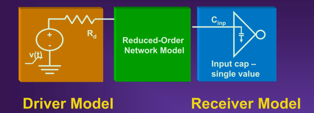
NLDM

nldm driver model

nldm表征的是cell的input到ouput的delay值以及输出的transition time。

如图,我们以一个反相器为例,在output load给定的情况下进行仿真的波形。红色的波形代表的是输入的激励,蓝色的波形代表的是通过仿真得到的输出的电压波形。

NLDM driver model characterization

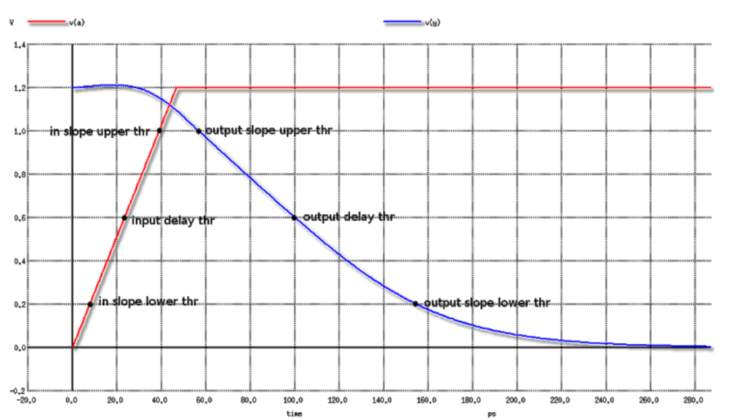
对于电压波形,nldm是通过三个点进行取样。三个点分别为delay threshold,transition threshold (upper & lower)。一个delay threshold指的是电压到 50% VDD的位置。而transition threshold,取值可能有所不同,有的用的是30% 70%,有的是20% 80% 。如果.lib用的组合不同,工具会自动进行换算。

那么图中的反相器的delay值,指的就是output delay threshold与input delay threshold的差值。

而output transition,则是output slop lower thr与output slop upper thr的差值。

那么,这两个值(delay,transition time),就用来构建NLDM driver model。如图所示:

NLDM driver model

在.lib文件中,nldm是一个二维查找表。这个查找表的两个index分别代表的是input transition,output load,如图所示。

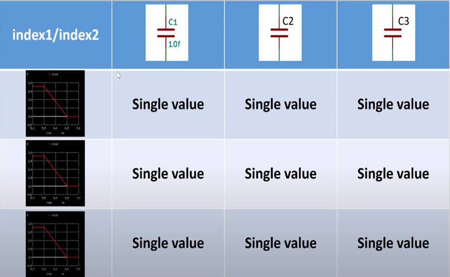
对于一个反相器,那么会有四个表格,两个分别表示的是上升沿和下降沿的delay 值, 另外两个则分别是上升沿和下降沿的transition time。

nldm receiver model

NLDM receiver model 是一个简单的电容。当然,上升沿和下降沿的电容是不同的。

nldm 遇到的问题

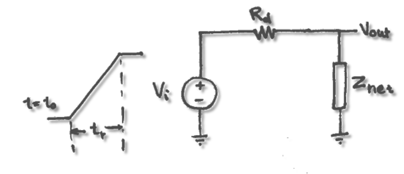
在65nm之前,NLDM相对准确。但是随着工艺尺寸的减少。金属连线上的电阻变得越来越大。一个典型的问题就是,当电压源内阻Rd远远小于net上的电阻的时候,电压源模型会严重失真。

而对于nldm receiver model,随着工艺尺寸的减少。miller效应越来越明显,单独的一个cap值已经无法正确表征真实情况,而这些效应在STA的计算中又非常的必不可少,尤其对于电阻小的的net尤为明显。

CCS

CCS model 很好的解决NLDM存在的这些问题。

同样,CCS也包括了CCS driver model和 CCS receiver model。

ccs driver model

CCS deiver model表征的是流入load cap的电路值。其参数同样是输入的transiton time以及输出的load。

CCS描述的是一个内部无限的电流源,因此,即使net的电阻非常大的情况,它也可以非常精确。

Figure: CCS (Composite Current Source) Driver Model

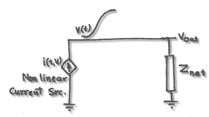
在.lib中,对应于不用的input transition以及output load,表中的值也不再是一个定值,而是电流的波形。

ccs receiver model

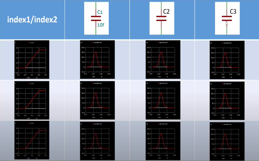
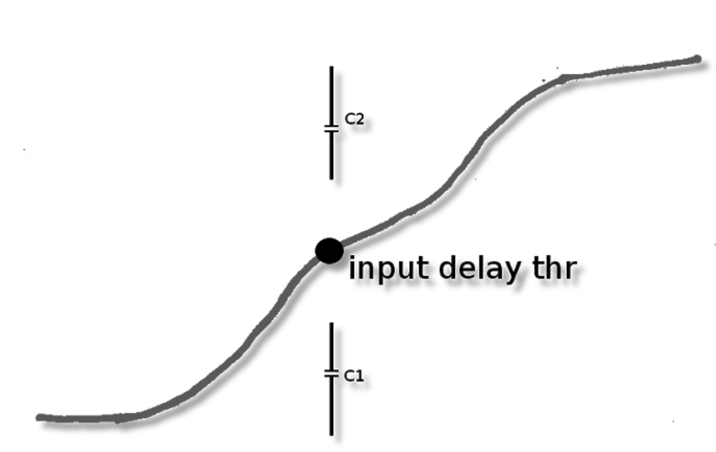
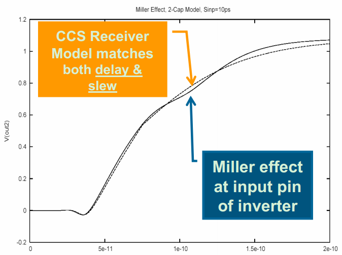
为了更精确的反应miller电容效应。model中用两个电容C1和C2来进行描述。

如图,在receiver的电压波形到达delay thereshold(50% vdd)之前时,用C1的值,而在到达delay threshold之后,则采用C2值。

Composite Current Source Receiver Model

这种效果怎么样的。这是CCS receiver model和spice仿真的对比图。

CCS vs spice

end

CCS中包括了CCS noise model,CCS power model。我们以后再进行介绍。

历史文章推荐:

千万门级芯片到底是多大规模?

当我们做后仿时我们究竟在仿些什么?

为什么需要对芯片的leakage功耗特别关注

为什么PrimeTime修timing时,带physical aware还不如不带physical aware

关于Virtual clock

physical_exclusive logical_exlusive asynchronous false_path 之总结

为什么异步时钟不要设false path

iming,timing,timing!Thatisthemainconcernofadigitaldesigner chargedwithdesigningasemiconductorchip.Whatisit,howisit described,andhowdoesoneverifyit?Thedesignteamofalarge digitaldesignmayspendmonthsarchitectinganditeratingthedesignto achievetherequiredtimingtarget.Besidesfunctionalverification,thetim- ingclosureisthemajormilestonewhichdictateswhenachipcanbere- leasedtothesemiconductorfoundryforfabrication.Thisbookaddresses thetimingverificationusingstatictiminganalysisfornanometerdesigns. Thebookhasoriginatedfrommanyyearsofourworkingintheareaof timingverificationforcomplexnanometerdesigns.Wehavecomeacross manydesignengineerstryingtolearnthebackgroundandvariousaspects ofstatictiminganalysis.Unfortunately,thereisnobookcurrentlyavail- ablethatcanbeusedbyaworkingengineertogetacquaintedwiththede- tailsofstatictiminganalysis.Thechipdesignerslackacentralreferencefor informationontiming,thatcoversthebasicstotheadvancedtimingverifi- cationproceduresandtechniques. Thepurposeofthisbookistoprovideareferenceforbothbeginnersas wellasprofessionalsworkingintheareaofstatictiminganalysis.Thebook T PREFACE xvi isintendedtoprovideablendoftheunderlyingtheoreticalbackgroundas wellasin-depthcoverageoftimingverificationusingstatictiminganaly- sis.Thebookcoverstopicssuchascelltiming,interconnect,timingcalcula- tion,andcrosstalk,whichcanimpactthetimingofananometerdesign.It describeshowthetiminginformationisstoredincelllibrarieswhichare usedbysynthesistoolsandstatictiminganalysistoolstocomputeandver- ifytiming. ThisbookcoversCMOSlogicgates,celllibrary,timingarcs,waveform slew,cellcapacitance,timingmodeling,interconnectparasiticsandcou- pling,pre-layoutandpost-layoutinterconnectmodeling,delaycalculation, specificationoftimingconstraintsforanalysisofinternalpathsaswellas IOinterfaces.Advancedmodelingconceptssuchascompositecurrent source(CCS)timingandnoisemodels,powermodelingincludingactive andleakagepower,andcrosstalkeffectsontimingandnoisearedescribed. Thestatictiminganalysistopicscoveredstartwithverificationofsimple blocksparticularlyusefulforabeginnertothisarea.Thetopicsthenextend tocomplexnanometerdesignswithconceptssuchasmodelingofon-chip variations,clockgating,half-cycleandmulticyclepaths,falsepaths,aswell astimingofsourcesynchronousIOinterfacessuchasforDDRmemoryin- terfaces.Timinganalysesatvariousprocess,environmentandinterconnect cornersareexplainedindetail.Usageofhierarchicaldesignmethodology involvingtimingverificationoffullchipandhierarchicalbuildingblocksis coveredindetail.Thebookprovidesdetaileddescriptionsforsettingup thetiminganalysisenvironmentandforperformingthetiminganalysisfor variouscases.Itdescribesindetailhowthetimingchecksareperformed andprovidesseveralcommonlyusedexamplescenariosthathelpillustrate theconcepts.Multi-modemulti-corneranalysis,powermanagement,as wellasstatisticaltiminganalysesarealsodescribed. Severalchaptersonbackgroundreferencematerialsareincludedintheap- pendices.TheseappendicesprovidecompletecoverageofSDC,SDFand SPEFformats.Thebookdescribeshowtheseformatsareusedtoprovide informationforstatictiminganalysis.TheSDFprovidescellandintercon- nectdelaysforadesignunderanalysis.TheSPEFprovidesparasiticinfor- mation,whicharetheresistanceandcapacitancenetworksofnetsina PREFACE xvii design.BothSDFandSPEFareindustrystandardsandaredescribedinde- tail.TheSDCformatisusedtoprovidethetimingspecificationsorcon- straintsforthedesignunderanalysis.Thisincludesspecificationofthe environmentunderwhichtheanalysismusttakeplace.TheSDCformatis adefactoindustrystandardusedfordescribingtimingspecifications. Thebookistargetedforprofessionalsworkingintheareaofchipdesign, timingverificationofASICsandalsoforgraduatestudentsspecializingin logicandchipdesign.Professionalswhoarebeginningtousestatictiming analysisorarealreadywell-versedinstatictiminganalysiscanusethis booksincethetopicscoveredinthebookspanawiderange.Thisbook aimstoprovideaccesstotopicsthatrelatetotiminganalysis,witheasy-to- readexplanationsandfiguresalongwithdetailedtimingreports. Thebookcanbeusedasareferenceforagraduatecourseinchipdesign andasatextforacourseintimingverificationtargetedtoworkingengi- neers.Thebookassumesthatthereaderhasabackgroundknowledgeof digitallogicdesign.Itcanbeusedasasecondarytextforadigitallogicde- signcoursewherestudentslearnthefundamentalsofstatictiminganalysis andapplyitforanylogicdesigncoveredinthecourse. Ourbookemphasizespracticalityandthoroughexplanationofallbasic conceptswhichwebelieveisthefoundationoflearningmorecomplextop- ics.Itprovidesablendoftheoreticalbackgroundandhands-onguideto statictiminganalysisillustratedwithactualdesignexamplesrelevantfor nanometerapplications.Thus,thisbookisintendedtofillavoidinthis areaforworkingengineersandgraduatestudents. ThebookdescribestimingforCMOSdigitaldesigns,primarilysynchro- nous;however,theprinciplesareapplicabletootherrelateddesignstyles aswell,suchasforFPGAsandforasynchronousdesigns.
评论 3
添加红包

请填写红包祝福语或标题

红包个数最小为10个

红包金额最低5元

当前余额3.43前往充值 >
需支付:10.00
成就一亿技术人!
领取后你会自动成为博主和红包主的粉丝 规则
hope_wisdom
发出的红包
实付
使用余额支付
点击重新获取
扫码支付
钱包余额 0

抵扣说明:

1.余额是钱包充值的虚拟货币,按照1:1的比例进行支付金额的抵扣。
2.余额无法直接购买下载,可以购买VIP、付费专栏及课程。

余额充值