


 本文详细介绍了在低功耗设计中使用UPF进行电源开关创建、电源状态管理和级联转换的过程,包括如何添加power switch、设置power state、创建power state group以及level shifter和retention的配置。并通过VCSNLP工具进行了仿真验证,探讨了开关实验、响应延迟、功耗状态和retention保存与恢复的细节。
例子中最初dut和环境见上篇low power-upf-vcsnlp(二)
例子中dut和环境在上篇基础上修改low power-upf-vcsnlp(三)
4.create_power_switch

-switch_type 指定switch类型,如果是粗粒度或者both,则output_supply_port必须指定否则报错。细粒度的则会忽略output_supply_port。
-output_supply_port指定output port name以及连接的net name
-input_supply_port指定input port name以及连接的net name
-control_port指定control port name和连接的net name。net负责开关的。
-on/off_state指定state,和对应的布尔表达式。
-ack_port -ack_delay指定响应port和延时。
(1)添加PD0的power switch
set_design_top top/dut_u
#create_power_domain PD_TOP -include_scope
create_power_domain PD_TOP -elements {.} \
-exclude_elements {inst0}
create_supply_port VDD_TOP
create_supply_port VSS_TOP
create_supply_net VDD_TOP
create_supply_net VSS_TOP
connect_supply_net VDD_TOP -ports VDD_TOP
connect_supply_net VSS_TOP -ports VSS_TOP
create_supply_set PD_TOP_SET \
-function {power VDD_TOP} \
-function {power VSS_TOP}
create_power_domain PD_TOP \
-supply {primary PD_TOP_SET} \
-update
create_supply_port VDD_TOP0
create_supply_net VDD_TOP0
connect_supply_net VDD_TOP0 -ports VDD_TOP0
#PD0
set_scope inst0
create_power_domain PD0 -elements {.}
create_supply_port VDD0_i
create_supply_port VSS0
create_supply_net VDD0_i
create_supply_net VSS0
#这个net是接到power switch中的output_supply_port上,并且作为PD0的supply_net.
create_supply_net VDD0_o
connect_supply_net VDD0_i -ports VDD0_i
connect_supply_net VSS0 -ports VSS0
create_power_switch PD0_SWITCH -domain PD0 \
-input_supply_port {in0 VDD0_i} \
-output_supply_port {out0 VDD0_o } \
-control_port {en0 pwr_en} \
-on_state {PD0_on in0 {en0}} \
-off_state {PD0_off {!en0}}
create_supply_set PD0_SET \
-function {power VDD0_o} \
-function {ground VSS0}
create_power_domain PD0 \
-supply {primary PD0_SET} \
-update
set_scope ..
connect_supply_net VSS_TOP -ports inst0/VSS0
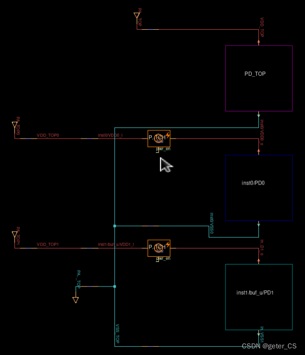
connect_supply_net VDD_TOP0 -ports inst0/VDD0_i仿真结果的power map如下,其中PD0的power supply port和power switch的 output supply port使用VDD0_o连接起来,power switch通过pwr_en进行控制:

(2)在增加一个PD1的power domain,并为其增加一个power switch。
set_design_top top/dut_u

#create_power_domain PD_TOP -include_scope
create_power_domain PD_TOP -elements {.} \
                -exclude_elements {inst0}

create_supply_port VDD_TOP
create_supply_port VSS_TOP
create_supply_net  VDD_TOP
create_supply_net  VSS_TOP

connect_supply_net VDD_TOP -ports VDD_TOP
connect_supply_net VSS_TOP -ports VSS_TOP

create_supply_set PD_TOP_SET \
    -function {power VDD_TOP} \
    -function {power VSS_TOP}

create_power_domain PD_TOP \
    -supply {primary PD_TOP_SET} \
    -update


create_supply_port VDD_TOP0
create_supply_net  VDD_TOP0
connect_supply_net VDD_TOP0 -ports VDD_TOP0

#PD0
set_scope inst0

create_power_domain PD0 -elements {.}

create_supply_port VDD0_i
create_supply_port VSS0

create_supply_net VDD0_i
create_supply_net VSS0

#这个net是接到power switch中的output_supply_port上,并且作为PD0的supply_net.
create_supply_net VDD0_o

connect_supply_net VDD0_i -ports VDD0_i
connect_supply_net VSS0 -ports VSS0

create_power_switch PD0_SWITCH -domain PD0 \
    -input_supply_port {in0 VDD0_i} \
    -output_supply_port {out0 VDD0_o } \
    -control_port {en0 pwr_en} \
    -on_state {PD0_on in0 {en0}} \
    -off_state {PD0_off {!en0}}

create_supply_set PD0_SET \
    -function {power VDD0_o}  \
    -function {ground VSS0}

create_power_domain PD0 \
    -supply {primary PD0_SET} \
    -update


set_scope ..

connect_supply_net VSS_TOP -ports inst0/VSS0
connect_supply_net VDD_TOP0 -ports inst0/VDD0_i

create_supply_port VDD_TOP1
create_supply_port VDD_TOP1
connect_supply_net VDD_TOP1 -ports VDD_TOP1


#PD1
set_scope inst1/buf_u

create_power_domain PD1 -elements {.}

create_supply_port VDD1_i
create_supply_port VSS1

create_supply_net VDD1_i
create_supply_net VSS1

create_supply_net VDD1_o

connect_supply_net VDD1_i -ports VDD1_i
connect_supply_net VSS1 -ports VSS1

create_power_switch PD1_SWITCH -domain PD1 \
    -input_supply_port {in1 VDD1_i} \
    -output_supply_port {out1 VDD1_o } \
    -control_port {en1 pwr_en} \
    -on_state {PD1_on in1 {en1}} \
    -off_state {PD1_off {!en1}}


create_supply_set PD1_SET \
    -function {power VDD1_o}  \
    -function {ground VSS1}

create_power_domain PD1 \
    -supply {primary PD1_SET} \
    -update


set_scope ..

connect_supply_net VSS_TOP -ports inst1/buf_u/VSS1
connect_supply_net VDD_TOP1 -ports inst1/buf_u/VDD1_i
仿真结果的power map如下,此时有三个power domain,PD_TOP,PD0,PD1,其中PD0和PD1都有power switch控制:
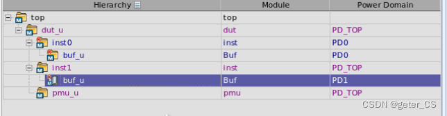
层次:
(3)power switch的开关实验。
我们将tb进行修改,将PD0和PD1的power switch进行开关,并分析波形。下面代码我们在520ns处将两个power en 拉低,在620ns时将PD1的power en打开,在720ns时将两个pwer en都打开。
`timescale 1ns/1ps

module top();
    import UPF::*;

    reg clk;
    reg rstn;
    reg [1:0] iso_en;
    reg [1:0] pwr_en;

    initial begin
        clk     = 0;
        rstn    = 0;
        iso_en  = 0;
        pwr_en  = 3;

        #20ns  rstn = 1;
        #400ns;
        #100ns pwr_en = 0;
        #100ns pwr_en = 2;
        #100ns pwr_en = 3;
        #100ns;
        $finish;
    end
    initial begin
        $fsdbDumpfile("top.fsdb");
        $fsdbDumpvars();
        $fsdbDumpvars("+power");
    end

    initial begin
        reg0=0;
        reg1=0;
        #100ns reg0 = 1;
        #100ns reg1 = 1;
        #200ns;

    end

    initial begin
        //supply
    end
    dut dut_u(.in0(reg0), .in1(reg1), .clk(clk), .rstn(rstn), .iso_en(iso_en), .pwr_en(pwr_en));
endmodule
波形结果如下,可以看到在掉电之后PD0,PD1 两个domain输出都是不定,所以需要加上isolation cell 防止这种不定输出对其他模块造成影响: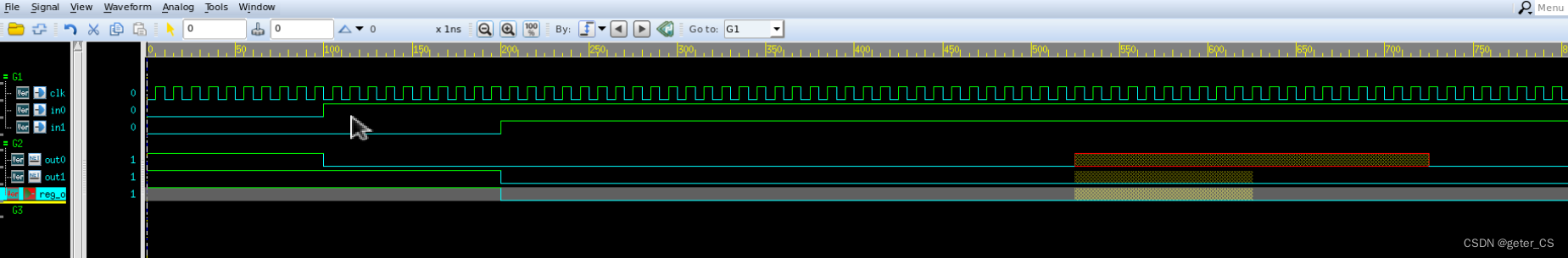
(3)把ack_port和ack_delay加上
我们在inst.v的inst端口上加一个pwr_ack信号,这个信号可以接出去。
module inst (input reg_i,input ido_en,input pwr_en,output reg_o,output pwr_ack);

    wire reg_o1 = ~reg_i;

    Buf buf_u(.in(reg_o1),.pwr_en(pwr_en).out(reg_o));

endmodule

module Buf(input in,input pwr_en,output out);
    assign out = in;
endmodule
然后在test.upf中对PD0加上ack_port和ack_delay。
set_design_top top/dut_u
#create_power_domain PD_TOP -include_scope
create_power_domain PD_TOP -elements {.} \
-exclude_elements {inst0}
create_supply_port VDD_TOP
create_supply_port VSS_TOP
create_supply_net VDD_TOP
create_supply_net VSS_TOP
connect_supply_net VDD_TOP -ports VDD_TOP
connect_supply_net VSS_TOP -ports VSS_TOP
create_supply_set PD_TOP_SET \
-function {power VDD_TOP} \
-function {power VSS_TOP}
create_power_domain PD_TOP \
-supply {primary PD_TOP_SET} \
-update
create_supply_port VDD_TOP0
create_supply_net VDD_TOP0
connect_supply_net VDD_TOP0 -ports VDD_TOP0
#PD0
set_scope inst0
create_power_domain PD0 -elements {.}
create_supply_port VDD0_i
create_supply_port VSS0
create_supply_net VDD0_i
create_supply_net VSS0
#这个net是接到power switch中的output_supply_port上,并且作为PD0的supply_net.
create_supply_net VDD0_o
connect_supply_net VDD0_i -ports VDD0_i
connect_supply_net VSS0 -ports VSS0
create_power_switch PD0_SWITCH -domain PD0 \
-input_supply_port {in0 VDD0_i} \
-output_supply_port {out0 VDD0_o } \
-control_port {en0 pwr_en} \
-on_state {PD0_on in0 {en0}} \
-off_state {PD0_off {!en0}} \
-ack_port {en_ack pwr_ack {en0}} \
-ack_delay {en_ack 10ns}
.......
......
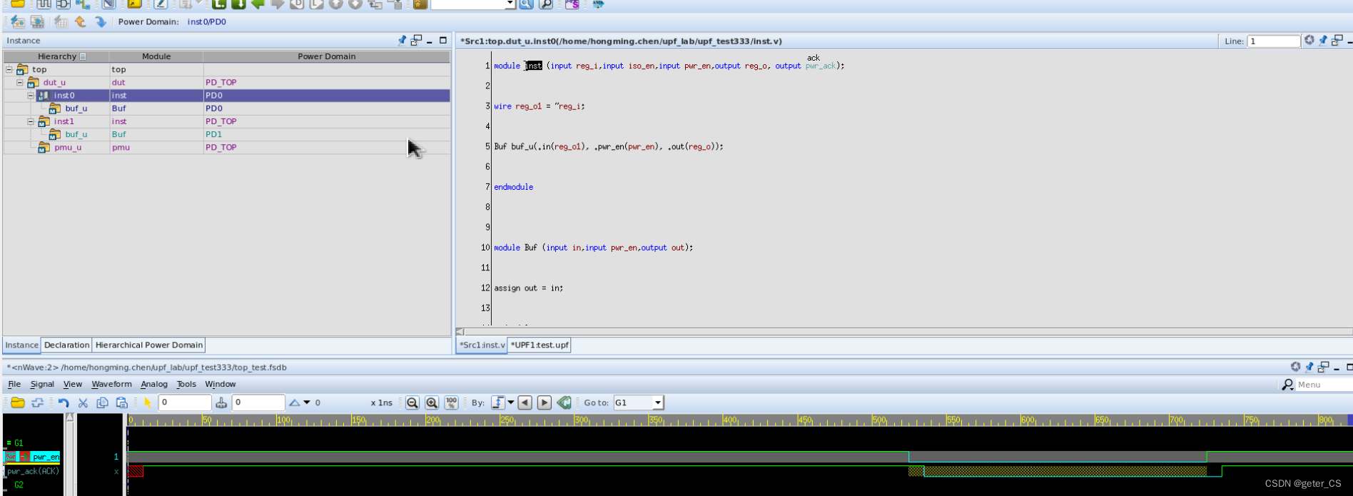
....然后其他不变,仿真波形如下,可以看见en_ack是pwr_en(也就算是port en0)的响应,而且响应的布尔表达式是en0,延时10ns,也就是en_ack和en0的值是一样的,并比en0晚10ns变化。并且注意代码窗口中inst0的pwr_ack上有ack的标志:
参考[0]:IEEE 1801-2015 IEEE Standard for Design and Verification of Low-Power, Energy-Aware Electronic Systems
verdi版本:R-2020.12-SP2
vcs版本: Q-2020.03-SP2
参考[1]: VCS Native Low Power (NLP)User Guide.
例子中最初dut和环境见上篇low power-upf-vcsnlp(二)
例子中dut和环境在上篇基础上修改来low power-upf-vcsnlp(五)
6.add_power_state
给supply_set的nets添加power states。然后在power state table中使用。
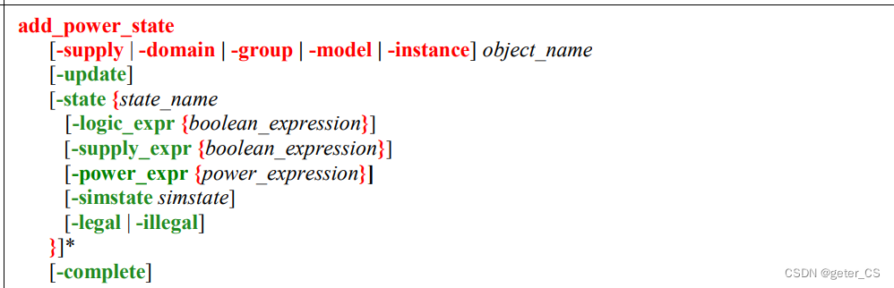
-supply_expr后面跟supply port/net/set的布尔表达式。
-logic_expr后面跟控制信号,时钟间隔,或者是已经定义好的object的power state的相关布尔表达式.([0]6.5.2)
-power_expr定义在此power state下的功耗,或者此power state下一个计算功耗的函数。
-simstate定义simstate,可以是NORMAL, CORRUPT_ON_CHANGE, CORRUPT_STATE_ON_CHANGE, CORRUPT_STATE_ON_ACTIVITY, CORRUPT_ON_ACTIVITY, CORRUPT, and NOT_NORMAL。波形上可以显示出来。
7.create_power_state_group
定义一个power state group name.
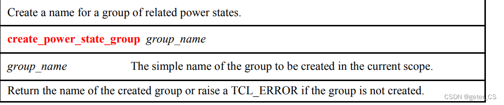
注意create_pst和add_pst_state是之前版本的命令。当然,IEEE1801-2015也是兼容这两个命令的。
在vcnlp中介绍了使用add_power_state定义一个power state table([1] P3-51):
a.使用-group指定一个group name
b.使用-state来指定power state table的state
c.使用-logic_expr来定义power state table的state的布尔表达式。
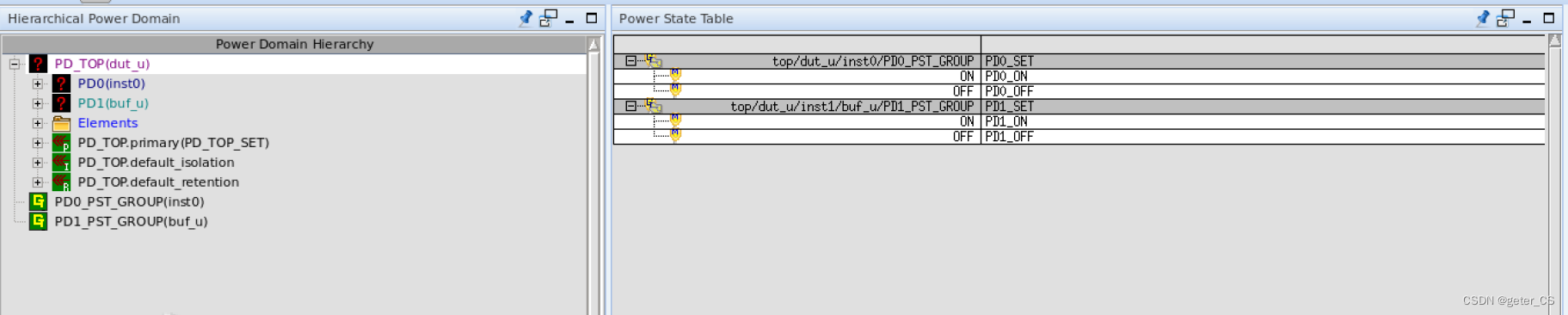
(1)添加PD0和PD1的PST.
基本代码和low power-upf-vcsnlp(五)一样的。注意add_power_state使用-group选项时,-state后使用的是-logic_expr来添加已经定义好的supply_set的state的布尔表达式。完整test.upf如下。
set_design_top top/dut_u

#create_power_domain PD_TOP -include_scope
create_power_domain PD_TOP -elements {.} \
                -exclude_elements {inst0}

create_supply_port VDD_TOP
create_supply_port VSS_TOP
create_supply_net  VDD_TOP
create_supply_net  VSS_TOP

connect_supply_net VDD_TOP -ports VDD_TOP
connect_supply_net VSS_TOP -ports VSS_TOP

create_supply_set PD_TOP_SET \
    -function {power VDD_TOP} \
    -function {power VSS_TOP}

create_power_domain PD_TOP \
    -supply {primary PD_TOP_SET} \
    -update


create_supply_port VDD_TOP0
create_supply_net  VDD_TOP0
connect_supply_net VDD_TOP0 -ports VDD_TOP0

#PD0
set_scope inst0

create_power_domain PD0 -elements {.}

create_supply_port VDD0_i
create_supply_port VSS0

create_supply_net VDD0_i
create_supply_net VSS0

#这个net是接到power switch中的output_supply_port上,并且作为PD0的supply_net.
create_supply_net VDD0_o

connect_supply_net VDD0_i -ports VDD0_i
connect_supply_net VSS0 -ports VSS0

create_power_switch PD0_SWITCH -domain PD0 \
    -input_supply_port {in0 VDD0_i} \
    -output_supply_port {out0 VDD0_o } \
    -control_port {en0 pwr_en} \
    -on_state {PD0_on in0 {en0}} \
    -off_state {PD0_off {!en0}} \
    -ack_port {en_ack pwr_ack {en0}} \
    -ack_delay {en_ack 10ns}

create_supply_set PD0_SET \
    -function {power VDD0_o}  \
    -function {ground VSS0}

create_power_domain PD0 \
    -supply {primary PD0_SET} \
    -update


set_scope ..

connect_supply_net VSS_TOP -ports inst0/VSS0
connect_supply_net VDD_TOP0 -ports inst0/VDD0_i

create_supply_port VDD_TOP1
create_supply_port VDD_TOP1
connect_supply_net VDD_TOP1 -ports VDD_TOP1


#PD1
set_scope inst1/buf_u

create_power_domain PD1 -elements {.}

create_supply_port VDD1_i
create_supply_port VSS1

create_supply_net VDD1_i
create_supply_net VSS1

create_supply_net VDD1_o

connect_supply_net VDD1_i -ports VDD1_i
connect_supply_net VSS1 -ports VSS1

create_power_switch PD1_SWITCH -domain PD1 \
    -input_supply_port {in1 VDD1_i} \
    -output_supply_port {out1 VDD1_o } \
    -control_port {en1 pwr_en} \
    -on_state {PD1_on in1 {en1}} \
    -off_state {PD1_off {!en1}}


create_supply_set PD1_SET \
    -function {power VDD1_o}  \
    -function {ground VSS1}

create_power_domain PD1 \
    -supply {primary PD1_SET} \
    -update


set_scope ..

connect_supply_net VSS_TOP -ports inst1/buf_u/VSS1
connect_supply_net VDD_TOP1 -ports inst1/buf_u/VDD1_i

#add isolation cell
set_isolation inst0_iso -domain inst0/PD0 \
        -elements  {inst0/reg_o[0]
                    inst0/reg_o1
                    } \
        -clamp_value 0 \
        -isolation_signal pmu_iso_en[0] \
        -isolation_supply PD_TOP_SET \
        -isolation_sense high \
        -location parent

#add power state PD0
set_scope inst0
add_power_state -supply PD0_SET \
    -state PD0_ON {-supply_expr {(power == {FULL_ON 1.0}) && (ground == {FULL_ON 0})} -simstate NORMAL} \
    -state PD0_OFF {-supply_expr {(power == {OFF 0.0}) && (ground == {FULL_ON 0})} -simstate CORRUPT}

#add power group PD0
create_power_state_group PD0_PST_GROUP
add_power_state -group PD0_PST_GROUP \
    -state ON {-logic_expr {PD0_SET == PD0_ON}} \
    -state OFF {-logic_expr {PD0_SET == PD0_OFF}}

set_scope ../
#add power state PD1
set_scope inst1/buf_u
add_power_state -supply PD1_SET \
    -state PD1_ON {-supply_expr {(power == {FULL_ON 1.8}) && (ground == {FULL_ON 0})} -simstate NORMAL} \
    -state PD1_OFF {-supply_expr {(power == {OFF 0.0}) && (ground == {FULL_ON 0})} -simstate CORRUPT}

#add power group PD1
create_power_state_group PD1_PST_GROUP
add_power_state -group PD1_PST_GROUP \
    -state ON {-logic_expr {PD1_SET == PD1_ON}} \
    -state OFF {-logic_expr {PD1_SET == PD1_OFF}}
仿真结果如下,可以看见两个group都已经显示在power table窗口上:
但是注意仿真的low power log中会有WARNING,警告如下:
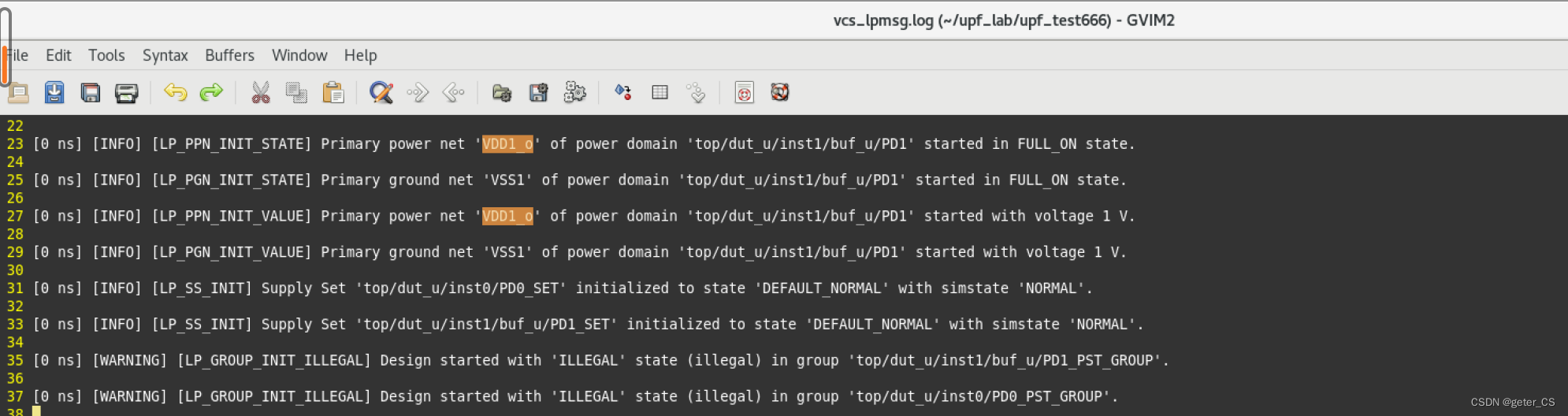
这是因为定义的state中指定了点电压,所以需要在top.sv中将对应的port supply on设置为对应的电压。注意设置电压不对,也会报错。supply_on/off需要添加import UPF:*。下图只展示top.sv中supply的代码,其余代码见low power-upf-vcsnlp(五)。注意PD0和PD1的供电分别来自于VDD_TOP0,VDD_TOP1。
    initial begin
        //supply
        supply_on("VDD_TOP0",1.0);
        supply_on("VDD_TOP1",1.8);
    end
    dut dut_u(.in0(reg0), .in1(reg1), .clk(clk), .rstn(rstn), .iso_en(iso_en), .pwr_en(pwr_en));
endmodule
此时进行仿真就不会有警告了。
![]()
(2)添加PD_TOP的PST.
在test.upf最后添加下面语句。
set_scope ../..
#add power state
add_power_state PD_TOP_SET -state P_ON {-supply_expr {power == {FULL_ON 0.8}}}
#add power group
create_power_state_group PD_TOP_PST_GROUP
add_power_state -group PD_TOP_PST_GROUP \
-state RUN {-logic_expr {(PD_TOP_SET == P_ON) && (inst0/PD0_PST_GROUP == ON) && (,inst1/buf_u/PD1_PST_GROUP == ON)}} \
-state IDLE {-logic_expr {(PD_TOP_SET == P_ON) && (inst0/PD0_PST_GROUP == ON) && (,inst1/buf_u/PD1_PST_GROUP == OFF)}} \
-state STOP {-logic_expr {(PD_TOP_SET == P_ON) && (inst0/PD0_PST_GROUP == OFF) && (,inst1/buf_u/PD1_PST_GROUP == ON)}} \
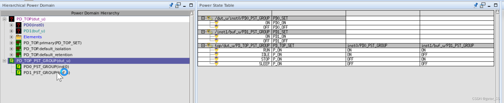
-state SLEEP {-logic_expr {(PD_TOP_SET == P_ON) && (inst0/PD0_PST_GROUP == OFF) && (,inst1/buf_u/PD1_PST_GROUP == OFF)}} 仿真结果,可以看见,PST中列出三个表,并且在power domain窗口中也显示出,PD_TOP_PST_GROUP将PD0和PD1的group包含了进去:
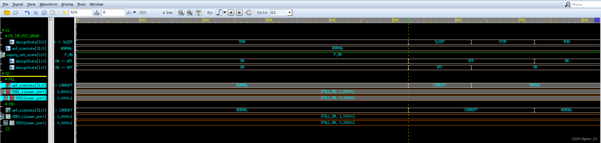
并且可以将power domain中的元素拉出到形上,如下图所示.可以展示出每个cycle各个PD所处的状态。
8.set_level_shifter
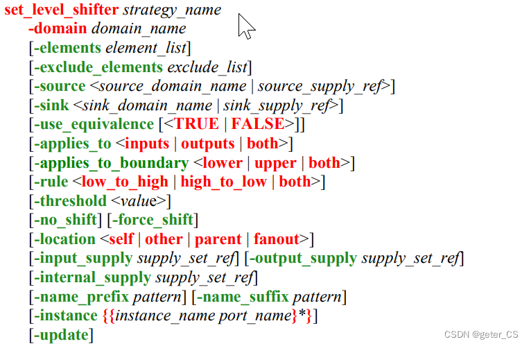
-elements指定此cell应用的ports或者instance.
-input_supply指定输入方的supply set.-output_supply指定输出方的supply set.
-location指定放置位置.默认是self.
-internal_supply指定cell内部电路的供电supply set.
-source,sink 通过这两个选项,支持基于路径的过滤。这两个选项后面跟supply set或者domain的名字。当是domain name时表示是这个domain的primary supply set.
-rule 指定cell应用于是low2high或者high2low方向的port,亦或者两者都可以。默认是both的。
-force_shift不使任何优化影响到level shift的设置。
注意这条命令会被vcsnlp解析并忽略。
(1).添加PD0和PD_TOP之间的level shifter.
test.upf在最后增加如下内容。
#add level shifter
set_level_shifter PD02PDTOP \
            -domain inst0/PD0 \
            -applies_to outputs \
            -input_supply PD0_SET \
            -output_supply PD_TOP_SET \
            -rule          both\
            -force_shift       \
            -location      parent

#add level shifter
set_level_shifter PDTOP2PD0 \
            -domain inst0/PD0 \
            -applies_to inputs \
            -input_supply PD_TOP_SET \
            -output_supply PD_SET \
            -rule          both\
            -force_shift       \
            -location      parent
仿真结果:
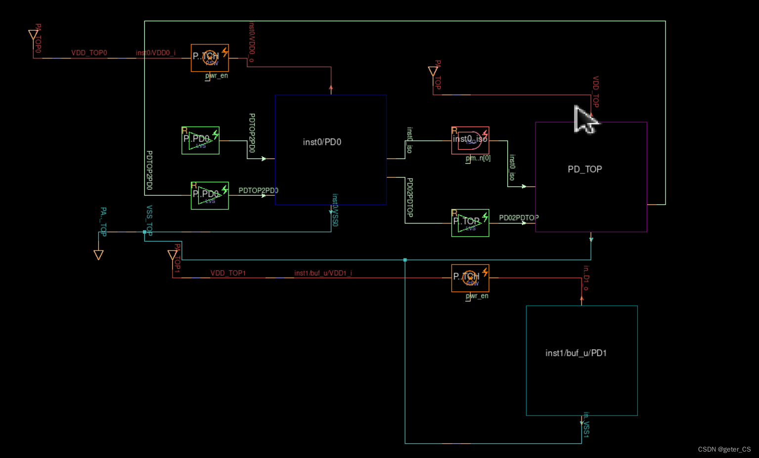
代码窗口会显示,被level shifter控制的signal:
(2)使用-applies_to both,也可以实现一样的效果.
#add level shifter
set_level_shifter PD02PDTOP \
            -domain inst0/PD0 \
            -applies_to both \
            -input_supply PD0_SET \
            -output_supply PD_TOP_SET \
            -rule          both\
            -force_shift       \
            -location      parent

#add level shifter
#set_level_shifter PDTOP2PD0 \
#            -domain inst0/PD0 \
#            -applies_to inputs \
#            -input_supply PD_TOP_SET \
#            -output_supply PD_SET \
#            -rule          both\
#            -force_shift       \
#            -location      parent
8.set_retention
(1)添加retention
如下这个例子,在intst.v中添加一个re_reg,并将clk和rstn也接进来,添加一个reg_t,只在做rst时赋值。在test.upf中将re_reg作为save_signal和restore_signal,把并设置为posedge和negedge。inst.v内容如下:
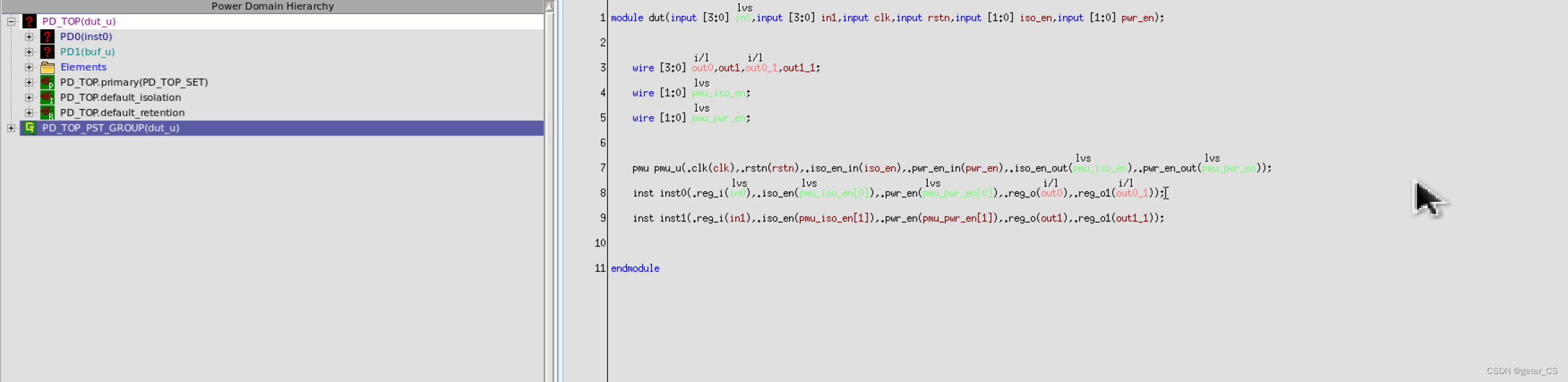
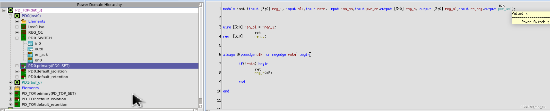
module inst (input clk,input rstn,input [3:0] reg_i,input iso_en,input pwr_en,output [3:0] reg_o, input re_reg, output [3:0] reg_o1, output pwr_ack);

    wire reg_o1 = ~reg_i;
    reg  [3:0] reg_t
    always @(posedge clk or negedge rstn)begin
        if(!rstn) begin
            reg_t<=9;
        end
    end
    Buf buf_u(.in(reg_o1),.pwr_en(pwr_en).out(reg_o));

endmodule

module Buf(input in,input pwr_en,output out);
    assign out = in;
endmodule
test.upf后面增加:
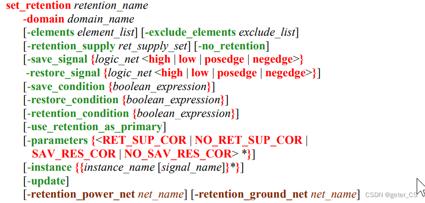
set_retention REG_O1 \
    -domain inst0/PD0 \
    -elements inst0/reg_t \
    -save_signal {inst0/re_reg posedge} \
    -restore_signal {inst0/re_reg negedge}
仿真结果的power domain的hierarchy中会显示设置的retention,代码窗口中也会给出ret标注:
波形上PD0掉电后在上电,reg_t为x态.
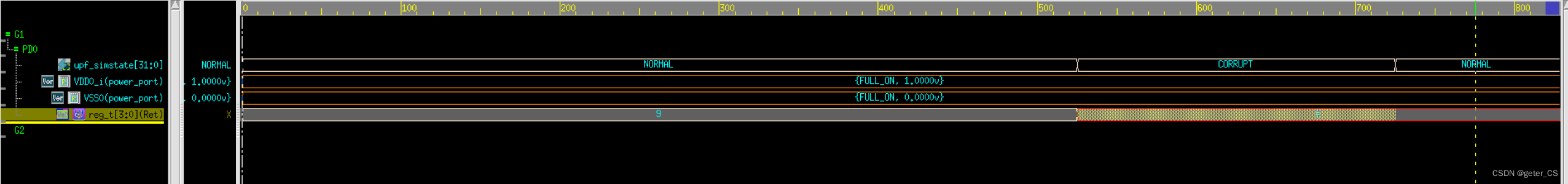
low power log中会给出warning.

(2)retention的save和restore
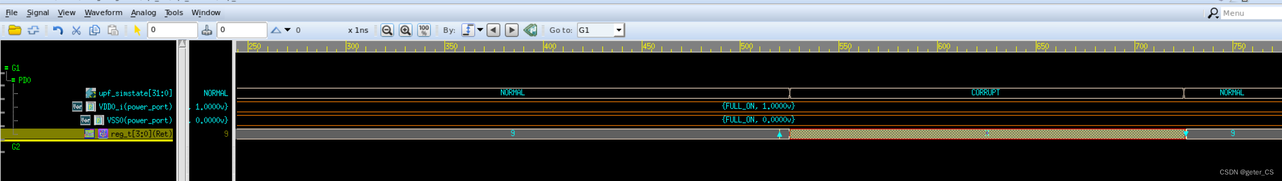
我们在top.sv加上对retention掉电前后的save和restore,就不会有上年面warning,并且在上电后,寄存器reg_t可以恢复掉电前状态。
修改top.sv如下,其余没写部分见上节low power-upf-vcsnlp(五):
`timescale 1ns/1ps

module top();
    import UPF::*;

    reg clk;
    reg rstn;
    reg [1:0] iso_en;
    reg [1:0] pwr_en;
    reg       re_reg;

    initial begin
        clk     = 0;
        rstn    = 0;
        iso_en  = 0;
        pwr_en  = 3;
        re_reg  = 0;

        #20ns  rstn = 1;
        #400ns;
        #100ns iso_en = 1;
               re_reg = 1;
               pwr_en = 0;
        #100ns pwr_en = 2;
        #100ns pwr_en = 3;
               iso_en = 0;
        #6ns;
               re_reg = 0;
        #100ns;
        $finish;
    end
    initial begin
        $fsdbDumpfile("top.fsdb");
        $fsdbDumpvars();
        $fsdbDumpvars("+power");
    end

.....
...
.
仿真结果波形,可以看见重新上电后reg_t恢复原值,且low power log中不在有警告:
参考[0]:IEEE 1801-2015 IEEE Standard for Design and Verification of Low-Power, Energy-Aware Electronic Systems
verdi版本:R-2020.12-SP2
vcs版本: Q-2020.03-SP2
参考[1]: VCS Native Low Power (NLP)User Guide.


 751
751


 到【灌水乐园】发言


