


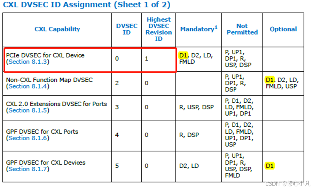
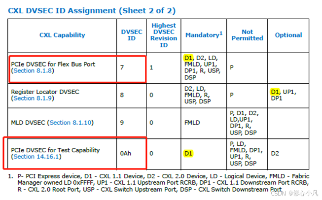
CXL 规范将配置空间寄存器分组为 **PCI Express 指定供应商特定扩展功能(DVSEC)** 结构,并通过 DVSEC Vendor ID 标识这些功能块。当 DVSEC Vendor ID 字段设置为 1E98h(版本 1)或 8086h(版本 0)时,表示该功能块由 CXL 规范定义。
二、贴一个cxl设备的配置空间寄存器的值:
  Type 0 Configuration Space Header
    Vendor ID    =    0x1B00  Montage
    Device ID    =    0xC000
    Cmd    =    0x0006
      IDSEL Stepping/Wait Cycle Control =     ........ 0.......  Off
      Parity Error Response =                 ........ .0......  Off
      VGA Palette Snoop =                     ........ ..0.....  Off
      Memory Write and Invalidate Enable =    ........ ...0....  Off
      Special Cycles Enable =                 ........ ....0...  Off
      Bus Master Enable =                     ........ .....1..  On
      Memory Space =                          ........ ......1.  On
      I/O Space =                             ........ .......0  Off
      Interrupt Disable =                     .....0.. ........  Off
      Fast Back-to-Back Transactions Enable = ......0. ........  Off
      SERR# Enable =                          .......0 ........  Off
    Status    =    0x0010
      Fast Back-to-Back Transactions Capable = ........ 0.......  Off
      66 MHz Capable =                         ........ ..0.....  Off
      Capabilities List =                      ........ ...1....  On
      Interrupt Pending =                      ........ ....0...  Off
      Immediate Readiness =                    ........ .......0  Off
      Detected Parity Error =                  0....... ........  Off
      Signaled System Error =                  .0...... ........  Off
      Received Master Abort =                  ..0..... ........  Off
      Received Target Abort =                  ...0.... ........  Off
      Signaled Target Abort =                  ....0... ........  Off
      DEVSEL Timing =                          .....00. ........  Fast
      Master Data Parity Error =               .......0 ........  Off
    Revision ID    =    0x01
    Class Code    =    0x050210  CXL memory device
    Cache Line Size    =    0  DWORDs
    Latency Timer    =    0
    Header Type    =    0x00  End point (single fct)
    BIST    =    0x00
      BIST Capable =    0... ....  Off
      Start BIST =      .0.. ....  Off
      Completion Code = .... 0000  Success
    BAR0    =    0x2000000C
      Base Address = 00100000 00000000 00000000 0000....  0x20000000
      Prefetchable = ........ ........ ........ ....1...  On
      Type =         ........ ........ ........ .....10.  64-bits
      SpcType =      ........ ........ ........ .......0  MemSpace
    BAR1    =    0x00000000
      Base Address = 00000000 00000000 00000000 0000....  0x00
      Prefetchable = ........ ........ ........ ....0...  Off
      Type =         ........ ........ ........ .....00.  32-bits
      SpcType =      ........ ........ ........ .......0  MemSpace
    BAR2    =    0x00000000
      Base Address = 00000000 00000000 00000000 0000....  0x00
      Prefetchable = ........ ........ ........ ....0...  Off
      Type =         ........ ........ ........ .....00.  32-bits
      SpcType =      ........ ........ ........ .......0  MemSpace
    BAR3    =    0x00000000
      Base Address = 00000000 00000000 00000000 0000....  0x00
      Prefetchable = ........ ........ ........ ....0...  Off
      Type =         ........ ........ ........ .....00.  32-bits
      SpcType =      ........ ........ ........ .......0  MemSpace
    BAR4    =    0x00000000
      Base Address = 00000000 00000000 00000000 0000....  0x00
      Prefetchable = ........ ........ ........ ....0...  Off
      Type =         ........ ........ ........ .....00.  32-bits
      SpcType =      ........ ........ ........ .......0  MemSpace
    BAR5    =    0x00000000
      Base Address = 00000000 00000000 00000000 0000....  0x00
      Prefetchable = ........ ........ ........ ....0...  Off
      Type =         ........ ........ ........ .....00.  32-bits
      SpcType =      ........ ........ ........ .......0  MemSpace
    Cardbus CIS Pointer    =    0x00000000
    Subsystem Vendor ID    =    0x0000
    Subsystem ID    =    0x0000
    ROMBase    =    0x00000000
      Base Address =         00000000 00000000 00000... ........  0x00
      Expansion ROM Enable = ........ ........ ........ .......0  Off
    Capabilities Pointer    =    0x40
    Interrupt Line    =    0xFF
    Interrupt Pin    =    0x00  No Legacy Interrupt Msg
    Min_Gnt    =    0  1/4 microseconds
    Max_Lat    =    0  1/4 microseconds
  PCI Power Management Capability
    PCICapHeader
      Capability ID    =    0x01  PCI Power Mgmt Interface
      Next Pointer    =    0x50
      PwrMgmtCaps    =    0x0003
        Device Specific Initialization =      ........ ..0.....  Off
        Immediate_Readiness_on_Return_to_D0 = ........ ...0....  Off
        PME Clock =                           ........ ....0...  Off
        Version =                             ........ .....011  v1.2
        PME# can be asserted from D3cold =    0....... ........  Off
        PME# can be asserted from D3hot =     .0...... ........  Off
        PME# can be asserted from D2 =        ..0..... ........  Off
        PME# can be asserted from D1 =        ...0.... ........  Off
        PME# can be asserted from D0 =        ....0... ........  Off
        D2_Support =                          .....0.. ........  Off
        D1_Support =                          ......0. ........  Off
        Aux_Current =                         .......0 00......  self powered
    PwrMgmtCtl/Status    =    0x0008
      No_Soft_Reset = ........ ....1...  On
      Power State =   ........ ......00  D0
      PME_Status =    0....... ........  Off
      Data_Scale =    .00..... ........  Unknown
      Data_Select =   ...0000. ........  D0 Power Consumed
      PME_En =        .......0 ........  Off
    PMCSR    =    0x00
      Bus Power/Clock Control Enable = 0... ....  Off
      B2/B3 support for D3hot =        .0.. ....  Off
    Data    =    0
  MSI Capability Structure
    PCICapHeader
      Capability ID    =    0x05  MSI
      Next Pointer    =    0x70
      Message Control    =    0x0186
        64 bit address capable =     ........ 1.......  On
        Multiple Message Enable =    ........ .000....  1 vector allocated
        Multiple Message Capable =   ........ ....011.  8 vectors requested
        MSI Enable =                 ........ .......0  Off
        Per-vector masking capable = .......1 ........  On
    Message Lower Address    =    0x00000000
    Message Upper Address    =    0x00000000
    Message Data    =    0x00000000
    Mask Bits    =    0x00000000
    Pending Bits    =    0x00000000
  PCI Express Capability Structure
    PCICapHeader
      Capability ID    =    0x10  PCIe
      Next Pointer    =    0xB0
      PCIe Capabilities Register    =    0x0002
        Device/Port Type =         ........ 0000....  PCI Express Endpoint
        Capability Version =       ........ ....0010  PCIe 3-4
        Interrupt Message Number = ..00000. ........  0x00
        Slot Implemented =         .......0 ........  Off
    Device Capabilities    =    0x10008FC0
      Extended Tag Field Supported =    ........ ........ ........ ..0.....  5-bit Tag
      Phantom Functions Supported =     ........ ........ ........ ...00...  No
      Max_Payload_Size Supported =      ........ ........ ........ .....000  128 bytes max pld
      Role-Based Error Reporting =      ........ ........ 1....... ........  On
      Endpoint L1 Acceptable Latency =  ........ ........ ....111. ........  No limit
      Endpoint L0s Acceptable Latency = ........ ........ .......1 11......  No limit
      Capture Slot Power Limit Value =  ......00 000000.. ........ ........  0
      ERR_COR Subclass Capable =        ........ .......0 ........ ........  Off
      Function Level Reset Capability = ...1.... ........ ........ ........  On
      Capture Slot Power Limit Scale =  ....00.. ........ ........ ........  1x
    Device Control    =    0x2010
      Max_Payload_Size =                         ........ 000.....  128 bytes max pld
      Enable Relaxed Ordering =                  ........ ...1....  On
      Unsupported Request Reporting Enable =     ........ ....0...  Off
      Fatal Error Reporting Enable =             ........ .....0..  Off
      Non-Fatal Error Reporting Enable =         ........ ......0.  Off
      Correctable Error Reporting Enable =       ........ .......0  Off
      BridgeConfigRetryEnable / Initiate Function Level Reset (FLR) = 0....... ........  Off
      Max_Read_Request_Size =                    .010.... ........  512 bytes max read
      Enable No Snoop =                          ....0... ........  Off
      Aux Power PM Enable =                      .....0.. ........  Off
      Phatom Functions Enable =                  ......0. ........  Off
      Extended Tag Field Enable =                .......0 ........  Off
    Device Status    =    0x0000
      Emergency Power Reduction Detected = ........ .0......  Off
      Transactions Pending =               ........ ..0.....  Off
      AUX Power Detected =                 ........ ...0....  Off
      Unsupported Request Detected =       ........ ....0...  Off
      Fatal Error Detected =               ........ .....0..  Off
      Non-Fatal Error Detected =           ........ ......0.  Off
      Correctable Error Detected =         ........ .......0  Off
    Link Capabilities    =    0x00436885
      Max Link Speed =                           ........ ........ ........ ....0101  32 GT/s
      L0s Exit Latency =                         ........ ........ .110.... ........  2 us-4 us
      ASPM Support =                             ........ ........ ....10.. ........  L1 Supported
      Max Link Width =                           ........ ........ ......00 1000....  8x
      ASPM Optionality Compliance =              ........ .1...... ........ ........  On
      Link Bandwidth Notification Capability =   ........ ..0..... ........ ........  Off
      Data Link Layer Link Active Reporting Capable = ........ ...0.... ........ ........  Off
      Surprise Down Error Reporting Capable =    ........ ....0... ........ ........  Off
      Clock Power Management =                   ........ .....0.. ........ ........  Off
      L1 Exit Latency =                          ........ ......11 0....... ........  0x0C
      Port Number =                              00000000 ........ ........ ........  0x00
    Link Control    =    0x0000
      Extended Synch =                           ........ 0.......  Off
      Common Clock Configuration =               ........ .0......  Off
      Retrain Link =                             ........ ..0.....  Off
      Link Disable =                             ........ ...0....  Off
      Read Completion Boundary =                 ........ ....0...  64 bytes
      ASPM Control =                             ........ ......00  Disabled
      DSR Signaling Control =                    00...... ........  DRS not Reported
      Link Autonomous Bandwidth Interrupt Enable = ....0... ........  Off
      Link Bandwidth Mgmt Interrupt Enable =     .....0.. ........  Off
      HW Autonomous Width Disable =              ......0. ........  Off
      Enable Clock Power Mgmt =                  .......0 ........  Off
    Link Status    =    0x1085
      Current Link Speed =               ........ ....0101  32 GT/s
      Link Autonomous Bandwidth Status = 0....... ........  Off
      Link Bandwidth Mgmt Status =       .0...... ........  Off
      Data Link Layer Link Active =      ..0..... ........  Off
      Slock Clock Configuration =        ...1.... ........  On
      Link Training =                    ....0... ........  Off
      Negotiated Link Width =            ......00 1000....  x8
    Slot Capabilities    =    0x00000000
      Hot-Plug Capable =                    ........ ........ ........ .0......  Off
      Hot-Plug Surprise =                   ........ ........ ........ ..0.....  Off
      Power Indicator Present =             ........ ........ ........ ...0....  Off
      Attention Indicator Present =         ........ ........ ........ ....0...  Off
      MRL Sensor Present =                  ........ ........ ........ .....0..  Off
      Power Controller Present =            ........ ........ ........ ......0.  Off
      Attention Button Present =            ........ ........ ........ .......0  Off
      Slot Power Limit Value =              ........ ........ .0000000 0.......  0
      No Command Completed Supported =      ........ .....0.. ........ ........  Off
      Electromechanical Interlock Present = ........ ......0. ........ ........  Off
      Slot Power Limit Scale =              ........ .......0 0....... ........  1x
      Physical Slot Number =                00000000 00000... ........ ........  0x00
    Slot Control    =    0x0000
      Attention Indicator Control =          ........ 00......  0x0
      Hot-Plug Interrupt Enable =            ........ ..0.....  Off
      Command Completed Interrupt Enable =   ........ ...0....  Off
      Presence Detected Changed Enable =     ........ ....0...  Off
      MRL Sensor Changed Enable =            ........ .....0..  Off
      Power Fault Detected Enable =          ........ ......0.  Off
      Attention Button Pressed Enable =      ........ .......0  Off
      In-Band PD Disable =
最低0.47元/天 解锁文章


 2483
2483

 被折叠的 条评论
为什么被折叠?
被折叠的 条评论
为什么被折叠?
 到【灌水乐园】发言


