


 这篇博客记录了一次大规模FPGA设计的综合过程,综合时间长达20分钟,远超以往。设计在综合后资源利用率较低,如Slice LUTs和Registers只占了极小比例,Block RAM Tile和DSP资源未被使用。由于某些部分的乘法结果未连接输出,导致被综合器删除。此外,设计被识别为空,可能因缺少输出接口。由于内存问题导致设计过程中电脑四次死机,解决方案是重构代码。
这里写自定义目录标题
前记
很长时间以来,我写的工程都是小规模的,综合时间大约5min以内(r7000p 2021),这次综合的时间是20min中,这是史无前例的,虽然我知道,综合时间这么长是因为我的HDL有问题。但是, 这个过程值得记录,用来后续的查阅。
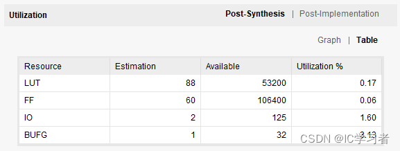
综合后的资源利用率
看起来波澜不惊,实际暗流涌动,因为乘法部分的结果没有连接输出,都被综合掉了。
synth_1_synth_report_utilization_0
Copyright 1986-2018 Xilinx, Inc. All Rights Reserved.
-------------------------------------------------------------------------------------------------
| Tool Version : Vivado v.2018.3 (win64) Build 2405991 Thu Dec  6 23:38:27 MST 2018
| Date         : Sat Apr 30 08:46:36 2022
| Host         : DESKTOP-FUK97V0 running 64-bit major release  (build 9200)
| Command      : report_utilization -file top_utilization_synth.rpt -pb top_utilization_synth.pb
| Design       : top
| Device       : 7z020clg400-1
| Design State : Synthesized
-------------------------------------------------------------------------------------------------

Utilization Design Information

Table of Contents
-----------------
1. Slice Logic
1.1 Summary of Registers by Type
2. Memory
3. DSP
4. IO and GT Specific
5. Clocking
6. Specific Feature
7. Primitives
8. Black Boxes
9. Instantiated Netlists

1. Slice Logic
--------------

+-------------------------+------+-------+-----------+-------+
|        Site Type        | Used | Fixed | Available | Util% |
+-------------------------+------+-------+-----------+-------+
| Slice LUTs*             |   88 |     0 |     53200 |  0.17 |
|   LUT as Logic          |   88 |     0 |     53200 |  0.17 |
|   LUT as Memory         |    0 |     0 |     17400 |  0.00 |
| Slice Registers         |   60 |     0 |    106400 |  0.06 |
|   Register as Flip Flop |   60 |     0 |    106400 |  0.06 |
|   Register as Latch     |    0 |     0 |    106400 |  0.00 |
| F7 Muxes                |    0 |     0 |     26600 |  0.00 |
| F8 Muxes                |    0 |     0 |     13300 |  0.00 |
+-------------------------+------+-------+-----------+-------+
* Warning! The Final LUT count, after physical optimizations and full implementation, is typically lower. Run opt_design after synthesis, if not already completed, for a more realistic count.


1.1 Summary of Registers by Type
--------------------------------

+-------+--------------+-------------+--------------+
| Total | Clock Enable | Synchronous | Asynchronous |
+-------+--------------+-------------+--------------+
| 0     |            _ |           - |            - |
| 0     |            _ |           - |          Set |
| 0     |            _ |           - |        Reset |
| 0     |            _ |         Set |            - |
| 0     |            _ |       Reset |            - |
| 0     |          Yes |           - |            - |
| 0     |          Yes |           - |          Set |
| 0     |          Yes |           - |        Reset |
| 0     |          Yes |         Set |            - |
| 60    |          Yes |       Reset |            - |
+-------+--------------+-------------+--------------+


2. Memory
---------

+----------------+------+-------+-----------+-------+
|    Site Type   | Used | Fixed | Available | Util% |
+----------------+------+-------+-----------+-------+
| Block RAM Tile |    0 |     0 |       140 |  0.00 |
|   RAMB36/FIFO* |    0 |     0 |       140 |  0.00 |
|   RAMB18       |    0 |     0 |       280 |  0.00 |
+----------------+------+-------+-----------+-------+
* Note: Each Block RAM Tile only has one FIFO logic available and therefore can accommodate only one FIFO36E1 or one FIFO18E1. However, if a FIFO18E1 occupies a Block RAM Tile, that tile can still accommodate a RAMB18E1


3. DSP
------

+-----------+------+-------+-----------+-------+
| Site Type | Used | Fixed | Available | Util% |
+-----------+------+-------+-----------+-------+
| DSPs      |    0 |     0 |       220 |  0.00 |
+-----------+------+-------+-----------+-------+


4. IO and GT Specific
---------------------

+-----------------------------+------+-------+-----------+-------+
|          Site Type          | Used | Fixed | Available | Util% |
+-----------------------------+------+-------+-----------+-------+
| Bonded IOB                  |    2 |     0 |       125 |  1.60 |
| Bonded IPADs                |    0 |     0 |         2 |  0.00 |
| Bonded IOPADs               |    0 |     0 |       130 |  0.00 |
| PHY_CONTROL                 |    0 |     0 |         4 |  0.00 |
| PHASER_REF                  |    0 |     0 |         4 |  0.00 |
| OUT_FIFO                    |    0 |     0 |        16 |  0.00 |
| IN_FIFO                     |    0 |     0 |        16 |  0.00 |
| IDELAYCTRL                  |    0 |     0 |         4 |  0.00 |
| IBUFDS                      |    0 |     0 |       121 |  0.00 |
| PHASER_OUT/PHASER_OUT_PHY   |    0 |     0 |        16 |  0.00 |
| PHASER_IN/PHASER_IN_PHY     |    0 |     0 |        16 |  0.00 |
| IDELAYE2/IDELAYE2_FINEDELAY |    0 |     0 |       200 |  0.00 |
| ILOGIC                      |    0 |     0 |       125 |  0.00 |
| OLOGIC                      |    0 |     0 |       125 |  0.00 |
+-----------------------------+------+-------+-----------+-------+


5. Clocking
-----------

+------------+------+-------+-----------+-------+
|  Site Type | Used | Fixed | Available | Util% |
+------------+------+-------+-----------+-------+
| BUFGCTRL   |    1 |     0 |        32 |  3.13 |
| BUFIO      |    0 |     0 |        16 |  0.00 |
| MMCME2_ADV |    0 |     0 |         4 |  0.00 |
| PLLE2_ADV  |    0 |     0 |         4 |  0.00 |
| BUFMRCE    |    0 |     0 |         8 |  0.00 |
| BUFHCE     |    0 |     0 |        72 |  0.00 |
| BUFR       |    0 |     0 |        16 |  0.00 |
+------------+------+-------+-----------+-------+


6. Specific Feature
-------------------

+-------------+------+-------+-----------+-------+
|  Site Type  | Used | Fixed | Available | Util% |
+-------------+------+-------+-----------+-------+
| BSCANE2     |    0 |     0 |         4 |  0.00 |
| CAPTUREE2   |    0 |     0 |         1 |  0.00 |
| DNA_PORT    |    0 |     0 |         1 |  0.00 |
| EFUSE_USR   |    0 |     0 |         1 |  0.00 |
| FRAME_ECCE2 |    0 |     0 |         1 |  0.00 |
| ICAPE2      |    0 |     0 |         2 |  0.00 |
| STARTUPE2   |    0 |     0 |         1 |  0.00 |
| XADC        |    0 |     0 |         1 |  0.00 |
+-------------+------+-------+-----------+-------+


7. Primitives
-------------

+----------+------+---------------------+
| Ref Name | Used | Functional Category |
+----------+------+---------------------+
| LUT2     |   61 |                 LUT |
| FDRE     |   60 |        Flop & Latch |
| LUT4     |   21 |                 LUT |
| CARRY4   |   20 |          CarryLogic |
| LUT3     |   18 |                 LUT |
| LUT6     |   12 |                 LUT |
| LUT1     |   11 |                 LUT |
| LUT5     |   10 |                 LUT |
| IBUF     |    2 |                  IO |
| BUFG     |    1 |               Clock |
+----------+------+---------------------+


8. Black Boxes
--------------

+-----------+------+
|  Ref Name | Used |
+-----------+------+
| ROM3_exp  |    1 |
| ROM2_VqIQ |    1 |
| ROM1_VpIQ |    1 |
+-----------+------+


9. Instantiated Netlists
------------------------

+----------+------+
| Ref Name | Used |
+----------+------+
[Common 17-1649]
[Common 17-1649] The Vivado message database 'F:/MyTest/FPGA/Correlation/Correlation.runs/synth_1/vivado.pb' contains 20871 messages.
Restoring all messages from this message database will impact Vivado performance, so only WARNING, CRITICAL WARNING, and ERROR messages will be restored.
To restore all messages from this file use the tcl command 'set_param messaging.loadPbLimit 20872' and re-open the project.
这里没显示的内容,应该可以到systhesized Design中的report找到
[Place 30-494] The design is empty
[Place 30-494] The design is empty
Resolution: Check if opt_design has removed all the leaf cells of your design.  Check whether you have instantiated and connected all of the top level ports.
[Common 17-69] Command failed: Placer could not place all instances
原因:顶层文件没有输出接口
因为内存爆掉死机了四次
解决方案,代码重写。
都看到这儿了,点个赞呗
||
\/


 2047
2047


 到【灌水乐园】发言


