


 本文介绍了如何使用Verilog语言在数字前端中通过时钟分频与倍频实现数据从宽到窄和从窄到宽的转换,并提供了相应的代码示例以及测试bench的实现。仿真结果显示了转换过程的工作原理。
#学习记录#
推荐阅读:数字前端-数据转换器(1)通过时钟分频与倍频实现数据位宽转换-优快云博客
1 由宽到窄数据转换
1.1 代码
`timescale 1ns / 1ps
//////////////////////////////////////////////////////////////////////////////////
// Company:
// Engineer: Mr-pn-junction
//
// Create Date: 2023/11/07 13:50:01
// Design Name:
// Module Name: wide_to_narrow
// Project Name:
// Target Devices:
// Tool Versions:
// Description:
//
// Dependencies:
//
// Revision:
// Revision 0.01 - File Created
// Additional Comments:
//
//////////////////////////////////////////////////////////////////////////////////


module wide_to_narrow(
    input clk2x,
    input rst_n,
    input clk1x,
    input [31:0] datain,
    output reg [31:0] datain_sync,
    output reg [15:0] dataout_clk2x,
    wire [15:0] dataout_clk2x_nxt
    );
always @(posedge clk2x or negedge rst_n)begin
    if(!rst_n)begin
    datain_sync <=0;
    dataout_clk2x <=0;
    end
    else
    datain_sync<=datain;
    end
assign dataout_clk2x_nxt = !clk1x?datain_sync[15:0] :datain_sync[31:16];
always @(posedge clk2x or negedge rst_n)begin
    if(!rst_n)begin
    datain_sync <=0;
    dataout_clk2x <=0;
    end
    else
    dataout_clk2x <= dataout_clk2x_nxt;
end
endmodule
1.2 testbench
`timescale 1ns / 1ps
//////////////////////////////////////////////////////////////////////////////////
// Company:
// Engineer: Mr-pn-junction
//
// Create Date: 2023/11/08 08:05:05
// Design Name:
// Module Name: wide_to_narrow_tb
// Project Name:
// Target Devices:
// Tool Versions:
// Description:
//
// Dependencies:
//
// Revision:
// Revision 0.01 - File Created
// Additional Comments:
//
//////////////////////////////////////////////////////////////////////////////////


module wide_to_narrow_tb(  );
    reg clk1x;
    reg clk2x;
    reg rst_n;
    reg [31:0] datain;
    wire [31:0] datain_sync;
    wire [15:0] dataout_clk2x;
wide_to_narrow tb(
    .clk1x(clk1x),
    .rst_n(rst_n),
    .clk2x(clk2x),
    .datain(datain),
    .datain_sync(datain_sync),
    .dataout_clk2x(dataout_clk2x)
    );
initial begin
    clk1x=0;clk2x=0;rst_n = 0;datain = 32'h0000_0000;
    #5
    rst_n = 1;datain = 32'h0000_0000;
    #20
    datain = 32'h1111_0000;
    #20
    datain = 32'h3333_2222;
    #20
    datain = 32'h5555_4444;
    #20
    datain = 32'h7777_6666;
    #40
    $stop;
end
always #5 clk2x = ~clk2x;
always #10 clk1x = ~clk1x;
endmodule
1.3 仿真结果
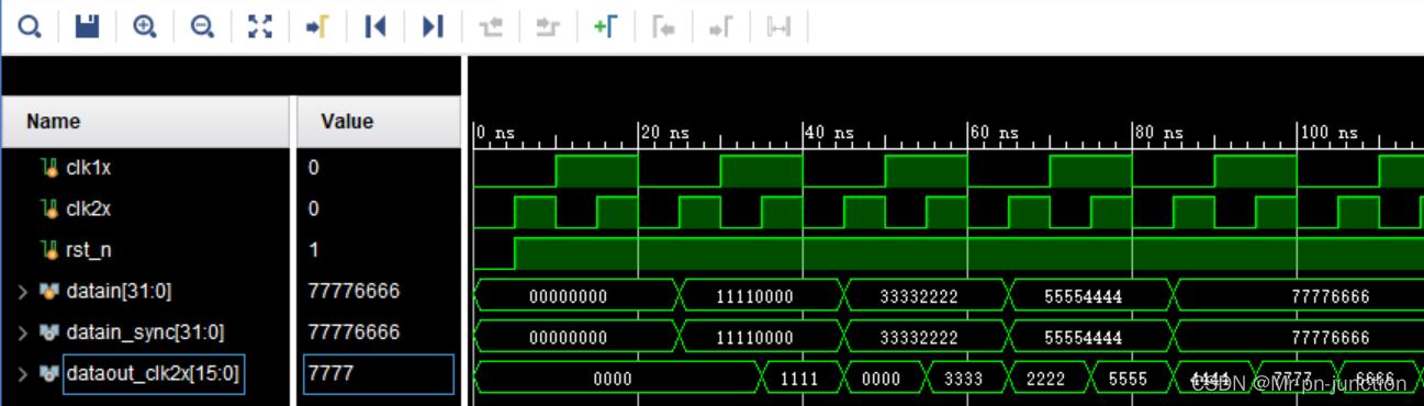
图1 仿真结果
2 由窄到宽数据转换
2.1 代码
module narrow_to_wide(
input clk2x,
input clk1x,
input [15:0] data16,
output reg [31:0] data32_clk1x
);
reg [15:0] data16_tmp;
reg [31:0] data32_clk1x_nxt;
always @(posedge clk2x) begin
data16_tmp <= #2data16;
end
assign data32_clk1x_nxt = {data16[15:0],data16_tmp[15:0]};
always @(posedge clk1x) begin
data32_clk1x <= data32_clk1x_nxt;
end
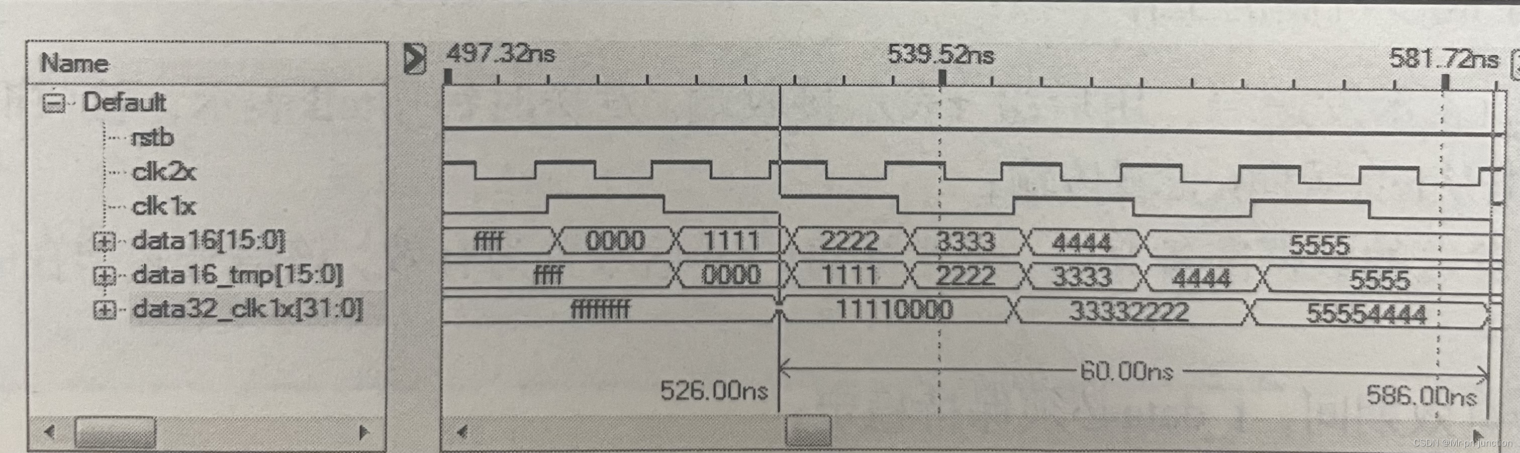
endmodule2.2 仿真结果
参考文献
[1] Verilog高级数字系统设计技术与实例分析. Kishore Mishra. 电子工业出版社.
[2] verilog手撕代码(7)数据位宽转换.Verilog手撕代码(7)数据位宽转换_verilog位宽转换_FPGA个人练习生的博客-优快云博客


 8846
8846

 被折叠的 条评论
为什么被折叠?
被折叠的 条评论
为什么被折叠?
 到【灌水乐园】发言


