


 本文详细介绍了NAND Flash的接口规范,包括CLE、ALE和WE_n信号的作用。在NV-DDR2和NV-DDR3接口中,这些信号用于区分命令、地址和数据的传输。写命令和写地址分别在特定的信号组合下被锁存,而写数据通过DQ总线由主机控制DQS_t和DQS_c的跳变进行。读数据时,主机通过RE_n信号触发,设备在固定延迟后将数据发送到DQ总线。
一、综述
nand flash的8个I/O(IO0 - IO7,在NV-DDR, NV-DDR2, and NV-DDR3规范里面又叫做DQ0-DQ7)是复用的,也就是说可以传数据,也可以传地址,也可以传命令。为了进行区分,引入了CLE(Command Latch Enable)、ALE(Address Latch Enable)两个管脚。
| CLE | ALE | DQ数据总线上的内容含义 |
| 高电平 | 低电平 | 命令 |
| 低电平 | 高电平 | 地址 |
| 低电平 | 低电平 | 数据 |
WE_n:
- The Write Enable signal controls the latching of commands, addresses, and input data in the SDR data interface.
- The Write Enable signal controls the latching of commands and addresses in the NV-DDR2 NV-DDR3 or NV-LPDDR4 data interface. Data, commands, and addresses are latched on the rising edge of WE_x_n.
- This signal shares the same pin as CLK_x in the NVDDR data interface.
RE_x_n/RE_x_c:
- The signal controls series data form device to host when the device is active.data is output at the both rising and falling edge of RE_n(NV-DDR2 NV-DDR3 or NV-LPDDR4 data interface)
- This signal shares the same pin as W/R_x_n in the NV-DDR data interface.
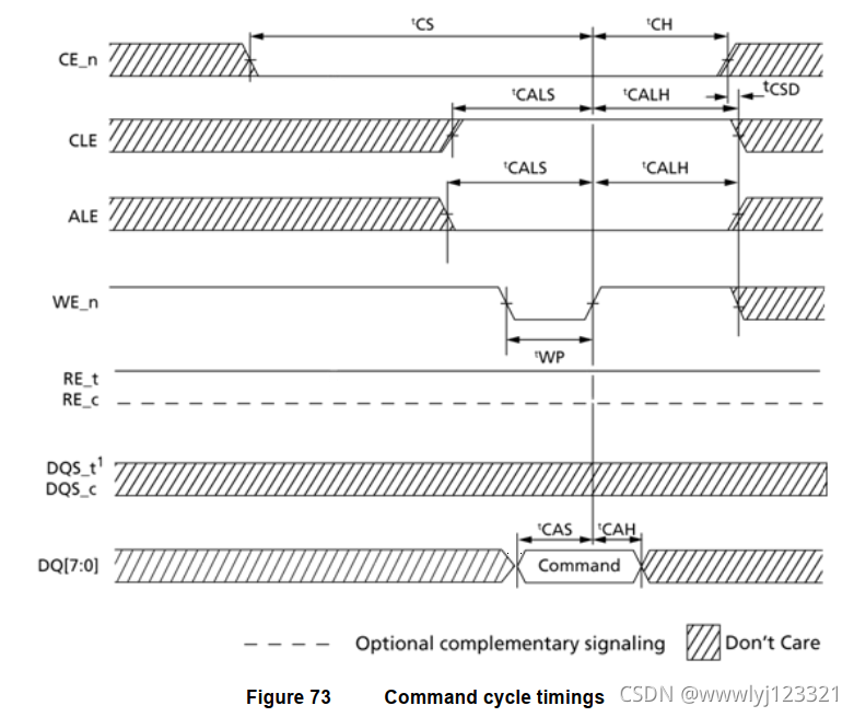
二、写命令
Command Information is latched by WE going ‘High’, when CE is ‘Low’, CLE is ‘High’, and ALE is ‘Low’
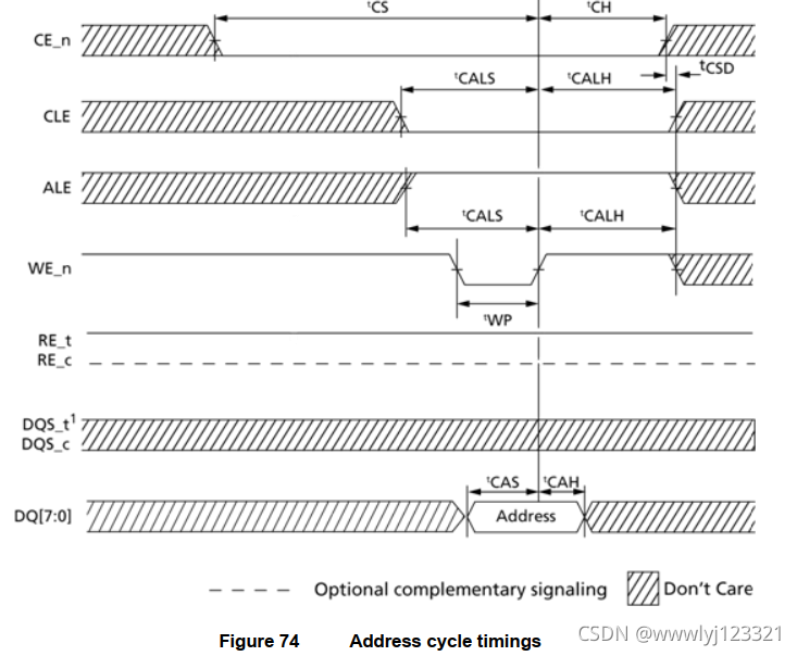
三、写地址
Address Information is latched by WE going ‘High’, when CE is ‘Low’, CLE is ‘Low’, and ALE is ‘High’.
四、写数据(host ---> nand flash)
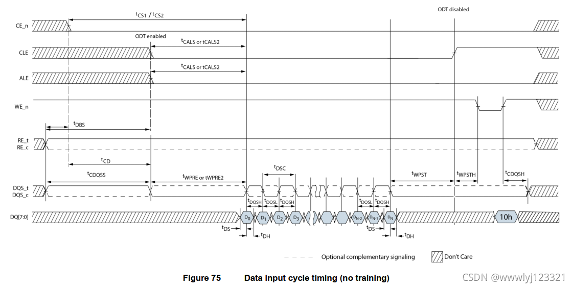
DQS_t和DQS_c是互补的,一个是高电平,另一个必然是低电平,也就是差分信号。
host控制着DQS和DQ总线,device在每一个DQS_t(DQS_c)的跳变沿进行采样,读取DQ总线host向flash发送的数据。
五、读数据
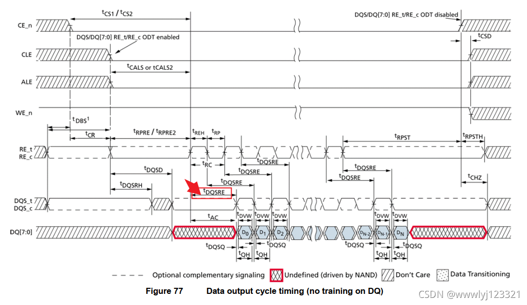
host控制RE_n(RE_c)线跳变(跳变多少次就说明主机要读几个字节),flash就知道host要读数据了,flash反应一段时间后(tDQSRE),就在将数据从DQ总线上发送出去。
从上图可以看出,host在DQ总线上第一次最佳的采样点为主机控制RE_n(RE_c)线跳变后tDQSRE+(tDQSQ+tDVW/2)。
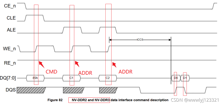
六、汇总
下面一个图总结了在nv-ddr2和nv-ddr3接口规范下,host发送cmd,address,data的逻辑图:
ref:


 2114
2114

 被折叠的 条评论
为什么被折叠?
被折叠的 条评论
为什么被折叠?
 到【灌水乐园】发言


