


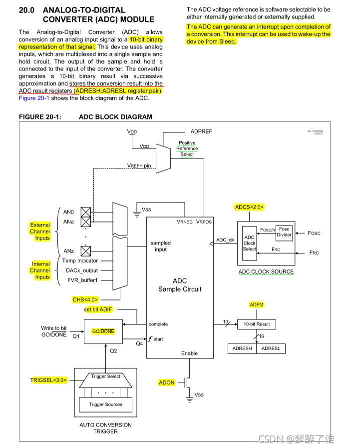
 这篇博客详细介绍了如何使用PIC16F15323单片机的ADC模块进行电压采集。首先,通过设置ADCON0和ADCON1寄存器来配置ADC,包括选择模拟输入通道、转换时钟源和参考电压。然后,通过编程启动AD转换并等待转换完成。转换完成后,读取ADRESH和ADRESL寄存器获取10位转换结果。同时,文章还展示了如何设置中断处理程序,用于检测AD转换完成。代码示例中,使用RA0作为模拟输入,RC0作为状态指示LED。
PIC16F15323单片机 (ADC)
1 基本原理
1.1 寄存器介绍
1.2 寄存器汇总
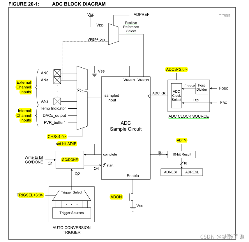
1.3 ADC采集实现框图
2 实现代码
/*---------------------------------函数功能:-------------------------------------
RA0(AN0)作为外部模拟电压的模拟输入口,并且用RC0口(LED)来判断电压采集是否完成,
如果AD采集完成,则AD对应的标志位ADIF=1,如果使能有效,则会产生一个中断,此时LED灯亮。
编程思路:参考手册的P131 To do an A/D Conversion, follow these steps
----------------------------------------------------------------------------*/
// PIC16F15323 Configuration Bit Settings
// 'C' source line config statements
// CONFIG1
#pragma config FEXTOSC = ECH // External Oscillator mode selection bits (EC above 8MHz; PFM set to high power)
#pragma config RSTOSC = EXT1X // Power-up default value for COSC bits (EXTOSC operating per FEXTOSC bits)
#pragma config CLKOUTEN = OFF // Clock Out Enable bit (CLKOUT function is disabled; i/o or oscillator function on OSC2)
#pragma config CSWEN = ON // Clock Switch Enable bit (Writing to NOSC and NDIV is allowed)
#pragma config FCMEN = ON // Fail-Safe Clock Monitor Enable bit (FSCM timer enabled)
// CONFIG2
#pragma config MCLRE = ON // Master Clear Enable bit (MCLR pin is Master Clear function)
#pragma config PWRTE = OFF // Power-up Timer Enable bit (PWRT disabled)
#pragma config LPBOREN = OFF // Low-Power BOR enable bit (ULPBOR disabled)
#pragma config BOREN = ON // Brown-out reset enable bits (Brown-out Reset Enabled, SBOREN bit is ignored)
#pragma config BORV = LO // Brown-out Reset Voltage Selection (Brown-out Reset Voltage (VBOR) set to 1.9V on LF, and 2.45V on F Devices)
#pragma config ZCD = OFF // Zero-cross detect disable (Zero-cross detect circuit is disabled at POR.)
#pragma config PPS1WAY = ON // Peripheral Pin Select one-way control (The PPSLOCK bit can be cleared and set only once in software)
#pragma config STVREN = ON // Stack Overflow/Underflow Reset Enable bit (Stack Overflow or Underflow will cause a reset)
// CONFIG3
#pragma config WDTCPS = WDTCPS_31// WDT Period Select bits (Divider ratio 1:65536; software control of WDTPS)
#pragma config WDTE = ON // WDT operating mode (WDT enabled regardless of sleep; SWDTEN ignored)
#pragma config WDTCWS = WDTCWS_7// WDT Window Select bits (window always open (100%); software control; keyed access not required)
#pragma config WDTCCS = SC // WDT input clock selector (Software Control)
// CONFIG4
#pragma config BBSIZE = BB512 // Boot Block Size Selection bits (512 words boot block size)
#pragma config BBEN = OFF // Boot Block Enable bit (Boot Block disabled)
#pragma config SAFEN = OFF // SAF Enable bit (SAF disabled)
#pragma config WRTAPP = OFF // Application Block Write Protection bit (Application Block not write protected)
#pragma config WRTB = OFF // Boot Block Write Protection bit (Boot Block not write protected)
#pragma config WRTC = OFF // Configuration Register Write Protection bit (Configuration Register not write protected)
#pragma config WRTSAF = OFF // Storage Area Flash Write Protection bit (SAF not write protected)
#pragma config LVP = ON // Low Voltage Programming Enable bit (Low Voltage programming enabled. MCLR/Vpp pin function is MCLR.)
// CONFIG5
#pragma config CP = OFF // UserNVM Program memory code protection bit (UserNVM code protection disabled)
// #pragma config statements should precede project file includes.
// Use project enums instead of #define for ON and OFF.
#include <xc.h>// 调用PIC16f15323单片机的头文件
//#include"delay.h"//调用延时子函数的头文件
/*-----------宏定义--------------*/
#define uint unsigned int
#define uchar unsigned char
uint ADbuf=0; // 缓存AD转换结果
/*-----------子函数声明--------------*/
/*-----------主函数--------------*/
void main()
{
//-------------------1、Configure Port:---------------------//
// The corresponding data direction register is TRISA.
// Setting a TRISA bit (= 1) will make the corresponding PORTA pi an input.
// Clearing a TRISA bit (= 0) will make the corresponding PORTA pin an output.
// 解释为什么需要TRISA0=1? After the A/D module has been configured as desired,
// the selected channel must be acquired before the conversion is started.
// The analog input channels must have their corresponding TRIS bits selected as inputs.
TRISA0=1; // RA0口为输入口,电压输入口
TRISC0=0; // AD响应中断对应的LED灯的数据方向为输出
// 1 = Port pin is > VIH,即高电平 ; 0 = Port pin is < VIL,即低电平
RA0=0; // 要不要这行语句没有影响,因为该端口是输入端口
RC0=0; // LED灯的初值为灭
//The ANSELA register (Register 14-4) is used to configure the Input mode of an I/O pin to analog.
// Setting the appropriate ANSE 如果ANSEL=1,IO口为模拟输入,如果ANSEL=0,数字IO口。
ANSA0=1; // Set RA0 to analog ANSELA0,为什么见头文件<xc.h>
while(1) // 死循环,单片机初始化后,就一直运行这个死循环
{
//-------------------2、Configure the ADC module:---------------------//
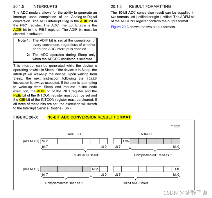
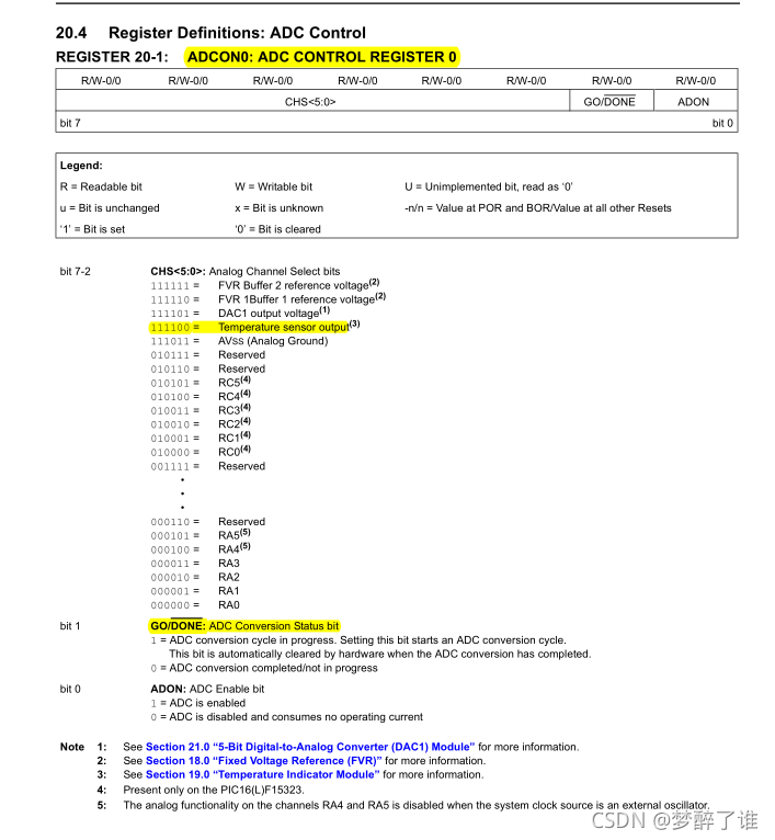
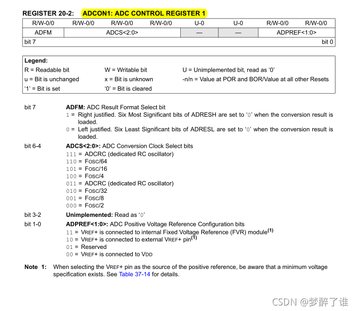
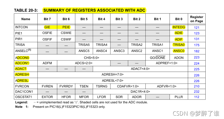
//(1)寄存器ADCON1: ADFM ADCS<2:0> - - ADPREF<1:0>
// 10-BIT ADC CONVERSION RESULT FORMAT
ADFM=1; // AD Result Format Select bit. 0 = Left justified. 1 = Right justified
//The source of the conversion clock is software selectable via the ADCS<2:0> bits
ADCS2=0;ADCS1=0;ADCS0=0; // Select ADC conversion clock FOSC/2
// The ADPREF<1:0> bits of the ADCON1 register provides control of the positive voltage reference
ADPREF1=0;ADPREF0=0; // Select voltage reference 00 =VREF+ is connected to VDD
//(2)寄存器ADCON0: CHS<5:0> GO/DONE ADON
//The CHS<5:0> bits of the ADCON0 register determine which channel is connected to the sample and hold circuit.
//CHS5=1;CHS4=1;CHS3=1;CHS2=1;CHS1=0;CHS0=0; // Select ADC input channel Temperature sensor 选择温度传感器作为模拟输入
CHS5=0;CHS4=0;CHS3=0;CHS2=0;CHS1=0;CHS0=0; // Select ADC input channel 选择RA0(AN0)作为模拟输入
//ADC Conversion Status bit. 1 = ADC conversion cycle in progress. Setting this bit starts an ADC conversion cycle.
// This bit is automatically cleared by hardware when the ADC conversion has completed.
// 0 = ADC conversion completed/not in progress
GOnDONE=0; // AD Conversion Status bit。为什么叫用GO_DONE看一下xc.h头文件
//To enable the ADC module, the ADON bit of the ADCON0 register must be set to a ‘1’.
ADON=1; //Turn on ADC module 模数转换器使能位。 1 = A/D converter module is powered up
//--------------------3、Configure ADC interrupt (optional):---------------------//
//ADIE=0; //禁止AD中断
//AD中断使能
ADIE=1;
ADIF=0; // Clear ADIF bit
INTEDG=1; // Interrupt Edge Select bit 1 = Interrupt on rising edge of INT pin
PEIE=1; // 允许外设中断
GIE=1; // 总中断允许
//----------ADC BLOCK DIAGRAM框图有下面两个寄存器,但是AD采集程序没有用到?--------------//
// AUTO CONVERSION TRIGGER
// TRIGSEL<3:0>;
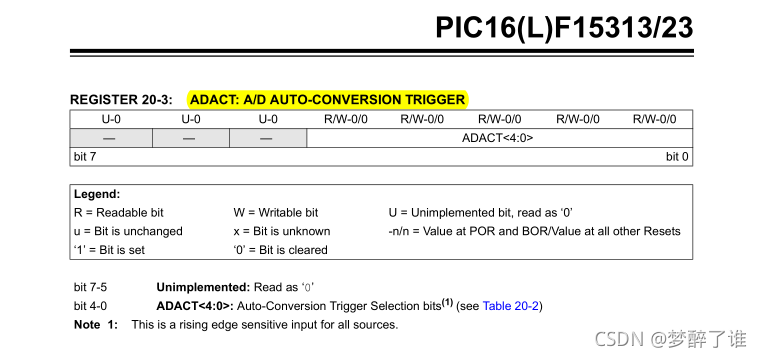
//The Auto-conversion Trigger source is selected with the ADACT<4:0> bits of the ADACT register.
ADACT4=0;ADACT3=0;ADACT2=0;ADACT1=0;ADACT0=0;//Auto-Conversion Trigger Selection bits
//--------------------4、 Wait the required acquisition time:---------------------//
asm("NOP"); //延时,让模拟电压稳定
asm("NOP");
asm("NOP");
asm("NOP");
asm("NOP");
//---------------5、Start conversion by setting the GO/DONE bit.:---------------------//
// When ADON = 1时,GO_DONE=1: AD conversion in progress set this bit(GO_DONE=1), starts the AD conversion.
// it is automatically cleared by hardware when the AD conversion is complete
GOnDONE=1; //开始进行AD转换 GO/DONE: A/D Conversion Status bit ADGO=1;
//---------6、Wait for ADC conversion to complete by one ofthe following:(1)Polling the GO/DONE bit。(2)Waiting for the ADC interrupt------//
while( GOnDONE) continue;//等待AD转换结束,AD转换完成后,GO_DONE自动由1变成0
//-----------------------7、Read ADC Result----------------------//
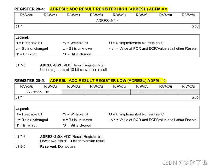
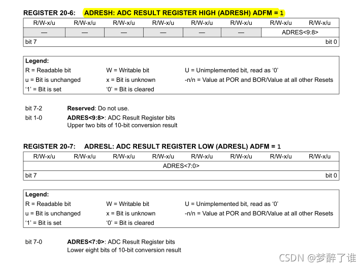
// The conversion of an analog input signal results in a corresponding 10-bit digital number.
// The ADRESH(高8位):ADRESL(低8位) registers contain the 10-bit result of the AD conversion.
// When the AD conversion is complete, the result is loaded into this AD Result register pair,
// and the GO/DONE bit is cleared and the A/D interrupt flag bit ADIF is set
// 需要注意到底是左对齐还是右对齐,这会影响ADbuf=ADRESH*256+ADRESL是否正确
ADbuf=ADRESH*256+ADRESL;//转换结果一共有10bit。由于2^10为1024,所以这是一个4位数 0-1023
//---------------8、Clear the ADC interrupt flag (required if interrupt is enabled)--------------------//
}
}
/*************中断服务程序***************/
// void __interrupt(irq(TMR0,TMR1),base(0x100)) timerIsr(void)
// 文档里可以查到要用 void __interrupt() ISR(void) 的形式添加中断程序
//void interrupt ISR(void)//PIC单片机的所有中断都是这样一个入口
void __interrupt() ISR(void)//PIC单片机的所有中断都是这样一个入口
{
// When the AD conversion is complete, the A/D interrupt flag bit ADIF is set.
if(ADIF==1) // 需要进一步判断是否为外部中断的溢出中断标志位
{
// The interrupt flag bit(s) must be cleared in software before
// re-enabling interrupts to avoid recursive interrupts
//溢出中断标志位清零 如果ADIF出现上升沿,则产生中断,所以中断发生之后要清零。
ADIF=0;
// 执行中断处理程序,执行中断产生时想要执行的功能
RC0=1; // 外部中断发生时,LED灯亮
}
}
/***********************************汇编语言**********************************/
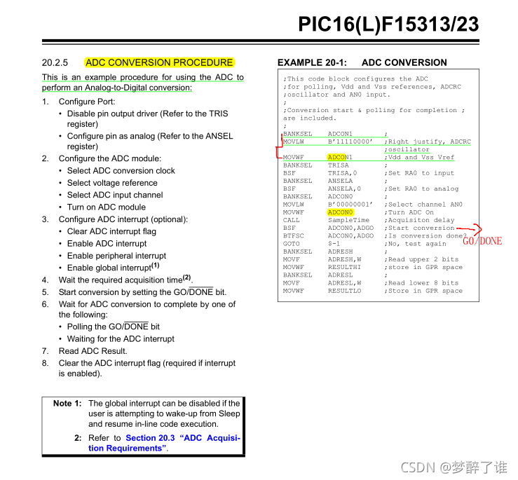
/*
BANKSEL ADCON1 ; //选择寄存器ADCON1
MOVLW B’11110000’; //将立即数11110000传送给工作寄存器W 功能:Right justify, ADCRC,oscillator; Vdd and Vss Vref
MOVWF ADCON1 ; //将W内的数据传送给ADCON1寄存器
BANKSEL TRISA ; //选择寄存器TRISA
BSF TRISA,0 ; //将TRISA第0位置1,即将端口RA0设置为输入 功能:Set RA0 to input
BANKSEL ANSELA ; //选择寄存器ANSELA
BSF ANSELA,0 ; //将ANSLA的第0位置1,即将端口RA0设置为模拟输入 功能:Set RA0 to analog
BANKSEL ADCON0 ; //选择寄存器ADCON0
MOVLW B’00000001’ ; //将立即数00000001传送给工作寄存器W 功能:Select channel AN0;ADC conversion cycle in progress. ; ADC is enabled
MOVWF ADCON0 ; //将W内的数据传送给ADCON0寄存器
CALL SampleTime ; // 延时 Acquisiton delay
BSF ADCON0,ADGO ; //将ADCON0的ADGO位置1,开始转换 功能:Start conversion ADC Conversion Status bit。1 = ADC conversion cycle in progress.
BTFSC ADCON0,ADGO ; //Is conversion done? 判断ADCON0的GO位是否为0? 为0则跳过,为1则顺序执行;
GOTO $-1 ; // No, test again 没有转换完成,再检测一遍
BANKSEL ADRESH ; //选择寄存器ADRESH
MOVF ADRESH,W ; // Read upper 2 bits 将高位ADRESH的数据存入W寄存器中
MOVWF RESULTHI ; //store in GPR space 将数据存储
BANKSEL ADRESL ; //选择寄存器ADRESL
MOVF ADRESL,W ; //Read lower 8 bits
MOVWF RESULTLO ; //Store in GPR space
*/


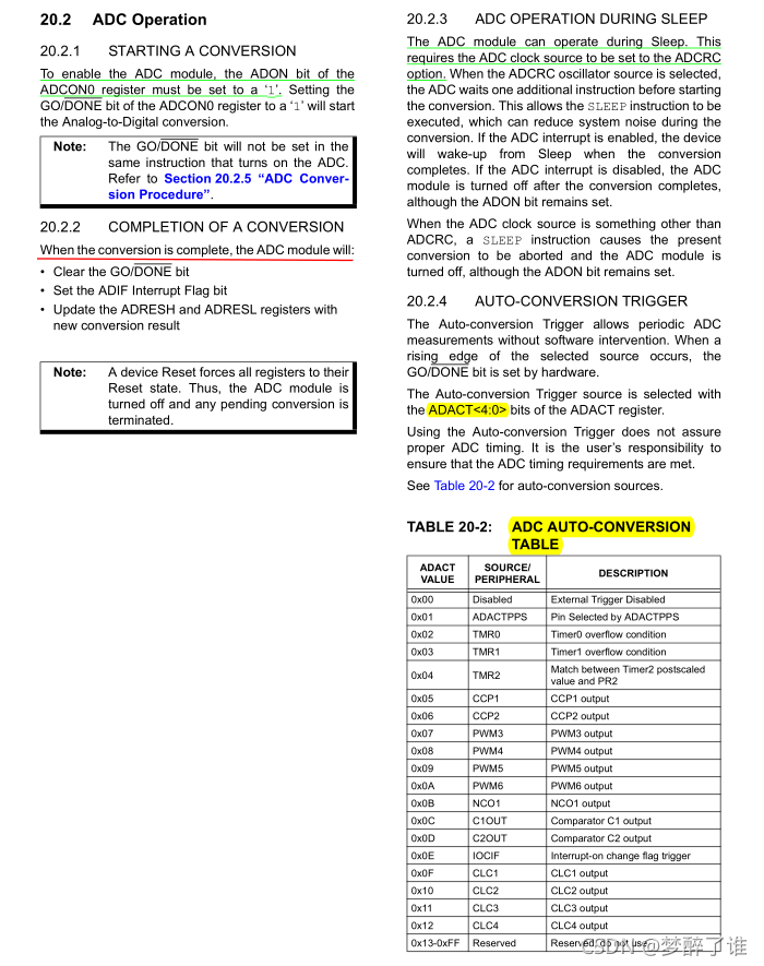
 1558
1558

 被折叠的 条评论
为什么被折叠?
被折叠的 条评论
为什么被折叠?
 到【灌水乐园】发言


