


 本文详细介绍了如何在PIC16F15323单片机上使用Timer0定时器进行中断操作,包括设置时钟源、预分频、后分频及中断配置,同时提供了清晰的代码示例,适合初学者理解和实践。
开发环境选择的是 MPLAB X IDE v5.50和 xc8-v2.32-full-install-windows-x64-installer。
1 基本原理
2 实现代码
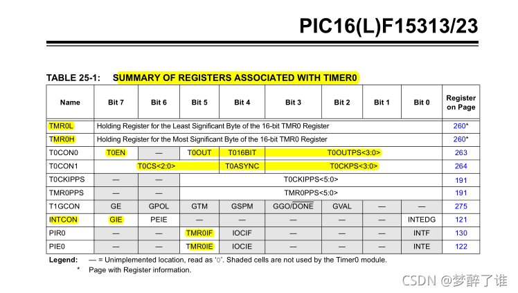
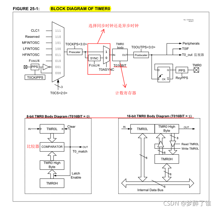
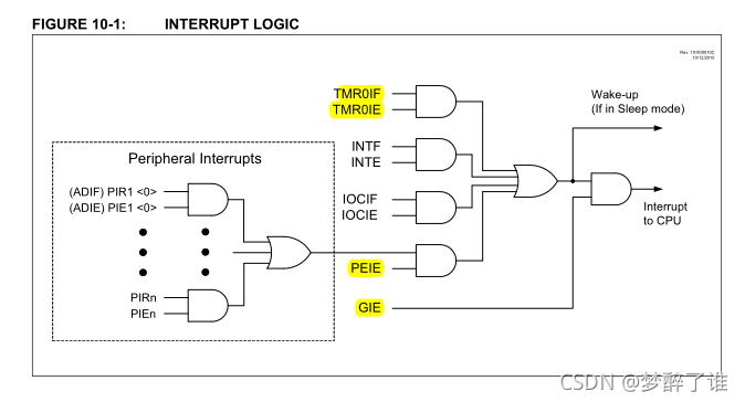
主要根据FIGURE 25-1 和中断的逻辑框图来编写代码,这样代码的可读性强,也便于理解。但有些寄存器在框图中可能没有说明,所以也需要仔细阅读定时器0的官方文档,即基本原理部分。
/*
* File: timer0.c
* Author: Sure
*---------------系统功能:
中断 定时器0
* Created on October 21, 2021, 7:48 PM
*/
// PIC16F15323 Configuration Bit Settings
// -----------熔丝配置--------------
// 'C' source line config statements
// CONFIG1
#pragma config FEXTOSC = ECH // External Oscillator mode selection bits (EC above 8MHz; PFM set to high power)
#pragma config RSTOSC = EXT1X // Power-up default value for COSC bits (EXTOSC operating per FEXTOSC bits)
#pragma config CLKOUTEN = OFF // Clock Out Enable bit (CLKOUT function is disabled; i/o or oscillator function on OSC2)
#pragma config CSWEN = OFF // Clock Switch Enable bit (Writing to NOSC and NDIV is allowed)
#pragma config FCMEN = OFF // Fail-Safe Clock Monitor Enable bit (FSCM timer enabled)
// CONFIG2
#pragma config MCLRE = OFF // Master Clear Enable bit (MCLR pin is Master Clear function)
#pragma config PWRTE = OFF // Power-up Timer Enable bit (PWRT disabled)
#pragma config LPBOREN = OFF // Low-Power BOR enable bit (ULPBOR disabled)
#pragma config BOREN = OFF // Brown-out reset enable bits (Brown-out Reset Enabled, SBOREN bit is ignored)
#pragma config BORV = LO // Brown-out Reset Voltage Selection (Brown-out Reset Voltage (VBOR) set to 1.9V on LF, and 2.45V on F Devices)
#pragma config ZCD = OFF // Zero-cross detect disable (Zero-cross detect circuit is disabled at POR.)
#pragma config PPS1WAY = OFF // Peripheral Pin Select one-way control (The PPSLOCK bit can be cleared and set only once in software)
#pragma config STVREN = OFF // Stack Overflow/Underflow Reset Enable bit (Stack Overflow or Underflow will cause a reset)
// CONFIG3
#pragma config WDTCPS = WDTCPS_31// WDT Period Select bits (Divider ratio 1:65536; software control of WDTPS)
#pragma config WDTE = OFF // WDT operating mode (WDT enabled regardless of sleep; SWDTEN ignored)
#pragma config WDTCWS = WDTCWS_7// WDT Window Select bits (window always open (100%); software control; keyed access not required)
#pragma config WDTCCS = SC // WDT input clock selector (Software Control)
// CONFIG4
#pragma config BBSIZE = BB512 // Boot Block Size Selection bits (512 words boot block size)
#pragma config BBEN = OFF // Boot Block Enable bit (Boot Block disabled)
#pragma config SAFEN = OFF // SAF Enable bit (SAF disabled)
#pragma config WRTAPP = OFF // Application Block Write Protection bit (Application Block not write protected)
#pragma config WRTB = OFF // Boot Block Write Protection bit (Boot Block not write protected)
#pragma config WRTC = OFF // Configuration Register Write Protection bit (Configuration Register not write protected)
#pragma config WRTSAF = OFF // Storage Area Flash Write Protection bit (SAF not write protected)
#pragma config LVP = OFF // Low Voltage Programming Enable bit (Low Voltage programming enabled. MCLR/Vpp pin function is MCLR.)
// CONFIG5
#pragma config CP = OFF // UserNVM Program memory code protection bit (UserNVM code protection disabled)
// #pragma config statements should precede project file includes.
// Use project enums instead of #define for ON and OFF.
#include <xc.h>//引用头文件
//#include"delay.h"//调用延时子函数
/*-----------宏定义--------------*/
#define uint unsigned int
#define uchar unsigned char
#define V0 RA0
uint i;
/*-----------子函数声明--------------*/
/*-----------主函数--------------*/
void main(void)
{
// The corresponding data direction register is TRISA.
// Setting a TRISA bit (= 1) will make the corresponding PORTA pi an input.
// Clearing a TRISA bit (= 0) will make the corresponding PORTA pin an output.
TRISA=0xfe; //设置数据方向 RA7-RA1为输入,RA0为输出
// 1 = Port pin is > VIH,即高电平 ; 0 = Port pin is < VIL ,即低电平
PORTA=0X00; //端口赋初值
/********定时器TMR0初始化**********/
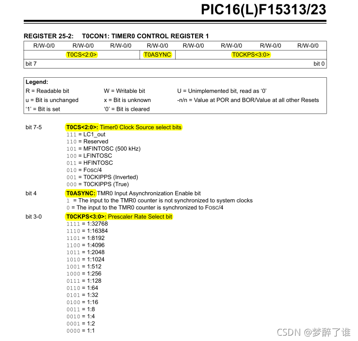
//The T0CS<2:0> bits of the T0CON1 register are used to select the clock source for Timer0.
// Clock Source Selection: 010 = FOSC/4
T0CS2=0; //TMR0时钟源选择位,TMR0的时钟源 选择 内部指令周期(fosc/4)
T0CS1=1;
T0CS0=0;
// There are 16 prescaler options for Timer0 ranging in powers of two from 1:1 to
// 1:32768. The prescaler values are selected using the T0CKPS<3:0> bits of the T0CON1 register.
T0CKPS3=0; // 预分频 1:1 ,对应的编码为0000
T0CKPS2=0;
T0CKPS1=0;
T0CKPS0=0;
// T0ASYNC: TMR0 Input Asynchronization Enable bit
// 1 = The input to the TMR0 counter is not synchronized to system clocks
// 0 = The input to the TMR0 counter is synchronized to FOSC/4
T0ASYNC=0; // 同步时钟模式
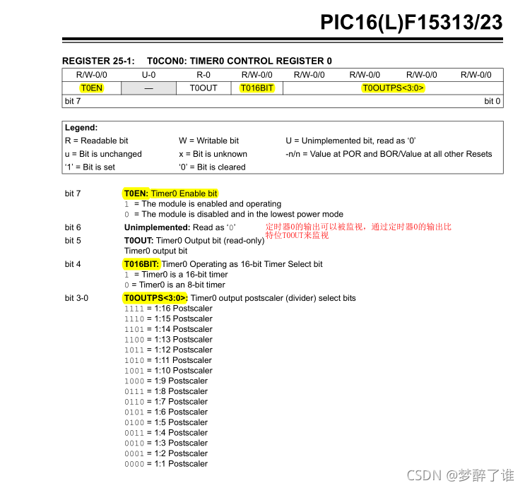
// T016BIT : Timer0 Operating as 16-bit Timer Select bit
// 1 = Timer0 is a 16-bit timer. 0 = Timer0 is an 8-bit timer
T016BIT=1; // 计数寄存器16位
// 2The Timer0 interrupt flag bit (TMR0IF) is set when either of the following conditions occur:
// 8-bit TMR0L matches the TMR0H value. 16-bit TMR0 rolls over from ‘FFFFh’
// The Timer1 module is a 16-bit timer/counter consisting of two 8-bit registers (TMR1H and TMR1L)
// which are readable and writable.
//16位计数寄存器给初值,在这里没有考虑中断所造成的时钟延迟13个指令周期
TMR0H=(65536-100)/256; // 定时100us*8(八分频),计数寄存器就会溢出
TMR0L=(65536-100)%256;
// There are 16 postscaler options for Timer0 ranging from 1:1 to 1:16.
// The postscaler values are selected using the T0OUTPS<3:0> bits of the T0CON0 register.
T0OUTPS3=0; // 后分频器 0000 = 1:1 Postscaler
T0OUTPS2=0;
T0OUTPS1=0;
T0OUTPS0=0;
// Timer0 Enable bit. 1 = The module is enabled and operating
// 0 = The module is disabled and in the lowest power mode
T0EN=1; // 打开定时器0
// This overflow sets bit TMR0IF(T0IF). 通过T0IF=1,来说明计数寄存器溢出了
TMR0IF=0; //TMR0的溢出中断标志位 清零,从而计数寄存器满的时候,T0IF产生一个上升沿。
//If Timer0 interrupts are enabled (TMR0IE bit of the PIE0 register = 1), the CPU will be interrupted
TMR0IE=1; // 打开定时器0的使能位
//******************** 开全局中断设置
//定时器T0设置了中断允许,此处要开全局中断
GIE=1; // 中断总允许控制位 置一
while(1) // 死循环,单片机初始化后,就一直运行这个死循环
{
}
}
/*************中断服务程序***************/
// void __interrupt(irq(TMR0,TMR1),base(0x100)) timerIsr(void)
// 文档里可以查到要用 void __interrupt() ISR(void) 的形式添加中断程序
//void interrupt ISR(void)//PIC单片机的所有中断都是这样一个入口
void __interrupt() ISR(void)//PIC单片机的所有中断都是这样一个入口
{
// The TMR0 interrupt is generated(T0IF==1) when the TMR0 register overflows from FFFFh to 0000h.
// 计数器寄存器由全1变为全0的时候,T0IF==1.
if(TMR0IF==1) //需要进一步判断是否为T0中断
{
//定时器中断后,要重置初值,以备下次中断
TMR0H=(65536-100)/256;
TMR0L=(65536-100)%256;
// Bit TMR0IF must be cleared in software by the Timer0 module Interrupt Service Routine
// before re-enabling this interrupt. 解释了为什么要清零
//溢出中断标志位清零 只有T0IF出现上升沿,才会产生中断,所以中断发生之后要清零。
TMR0IF=0;
// 执行中断处理程序,也就是中断产生了,我们想要执行什么功能
if(++i>250) //2ms中断一次,再计次250次后就是500ms
{
i=0;
V0=!V0; // 取反 实现一秒的闪烁
}
}
}


 906
906

 被折叠的 条评论
为什么被折叠?
被折叠的 条评论
为什么被折叠?
 到【灌水乐园】发言


