


 该文详细描述了在DCLAB4基础上修改的时序约束,包括时钟定义、输入时序、输出时序、组合逻辑时序以及环境属性。新增的约束选项涉及负边沿输入和输出时序。文章还概述了DCflow的执行步骤,如读入设计、约束、编译和报告等,用于验证和优化设计时序。
1.constraints(在DC LAB4的基础上进行修改)
1.1 CLOCK DEFINITION
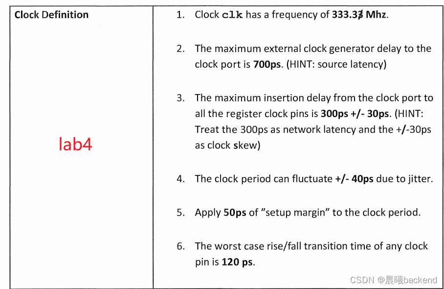
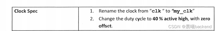
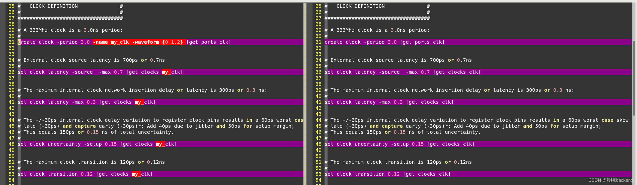
# A 333Mhz clock is a 3.0ns period:
#
create_clock -period 3.0 -name my_clk -waveform {0 1.2} [get_ports clk]

# External clock source latency is 700ps or 0.7ns
#
set_clock_latency -source  -max 0.7 [get_clocks my_clk]

# The maximum internal clock network insertion delay or latency is 300ps or 0.3 ns:
#
set_clock_latency -max 0.3 [get_clocks my_clk]

# The +/-30ps internal clock delay variation to register clock pins results in a 60ps worst case skew or uncertainty,
#if you launch late (+30ps) and capture early (-30ps)r;
#Add 40ps due to jitter and 50ps for setup margin;
# This equals 150ps or 0.15 ns of total uncertainty.
#
set_clock_uncertainty -setup 0.15 [get_clocks my_clk]


# The maximum clock transition is 120ps or 0.12ns
#
set_clock_transition 0.12 [get_clocks my_clk]
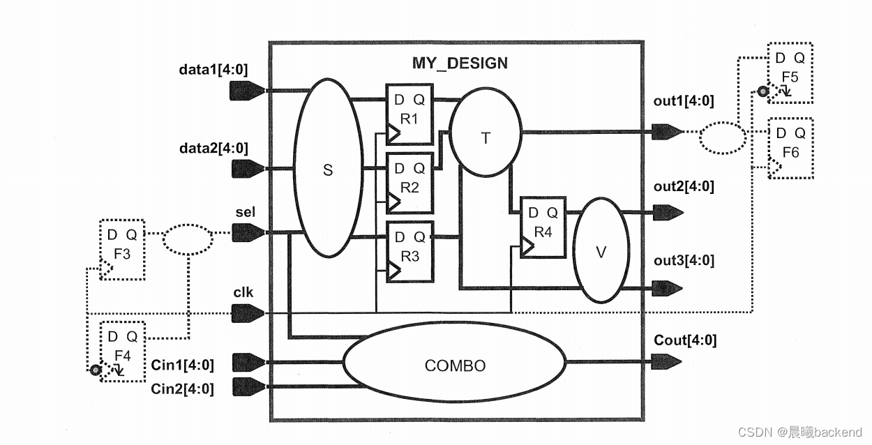
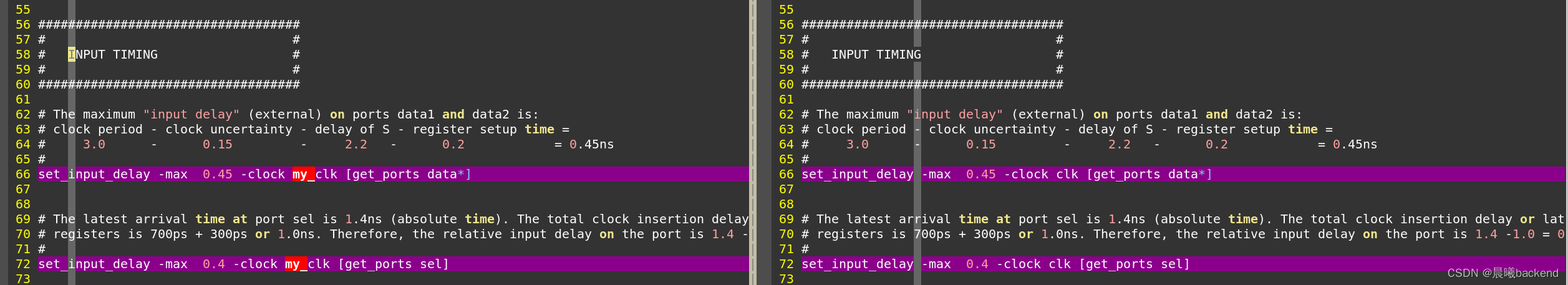
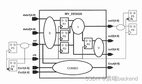
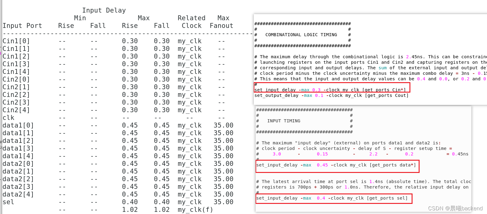
1.2 INPUT TIMING
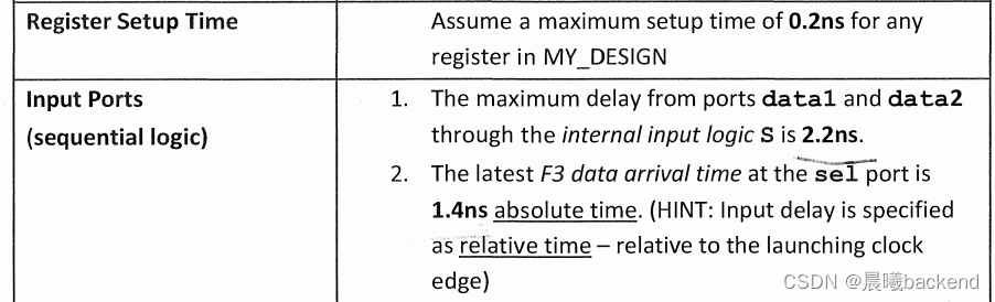
# The maximum "input delay" (external) on ports data1 and data2 is:
# clock period - clock uncertainty - delay of S - register setup time =
#     3.0      -      0.15         -     2.2   -      0.2            = 0.45ns
#
set_input_delay -max  0.45 -clock my_clk [get_ports data*]


# The latest arrival time at port sel is 1.4ns (absolute time). The total clock insertion delay or latency to the external
# registers is 700ps + 300ps or 1.0ns. Therefore, the relative input delay on the port is 1.4 -1.0 = 0.4ns
#
set_input_delay -max  0.4 -clock my_clk [get_ports sel]
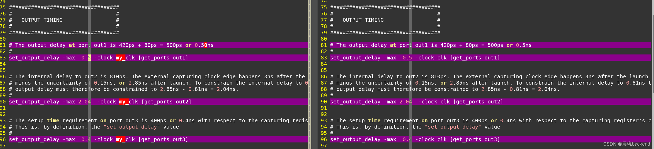
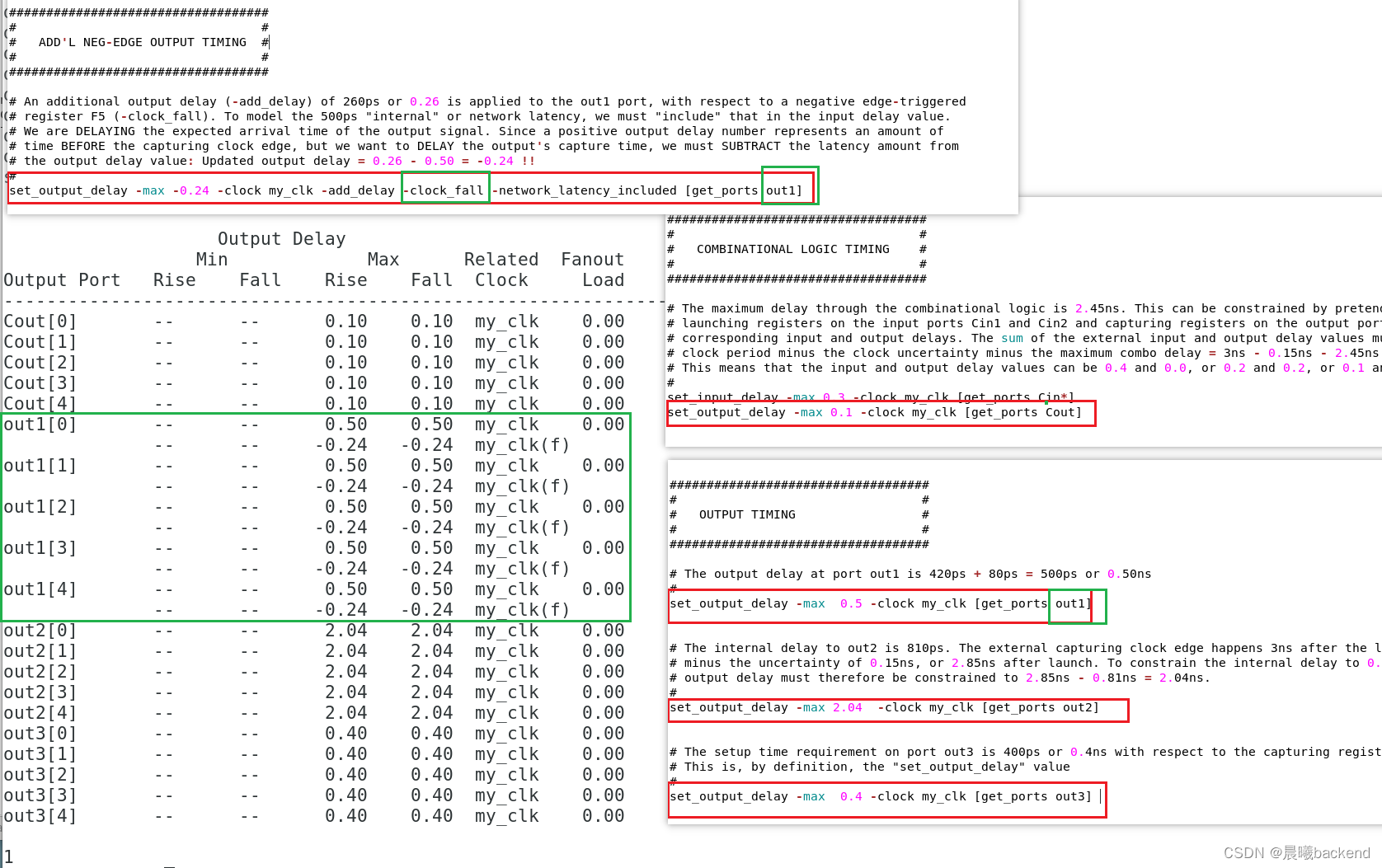
1.3 OUTPUT TIMING
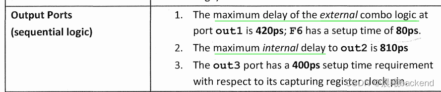
# The output delay at port out1 is 420 + 80ps = 500ps or 0.50ns
#
set_output_delay -max  0.50 -clock my_clk [get_ports out1]


# The internal delay to out2 is 810ps. The external capturing clock edge happens 3ns after the launch edge,
# minus the uncertainty of 0.15ns, or 2.85ns after launch. To constrain the internal delay to 0.81ns the
# output delay must therefore be constrained to 2.85ns - 0.81ns = 2.04ns.
#
set_output_delay -max 2.04  -clock my_clk [get_ports out2]


# The setup time requirement on port out3 is 400ps or 0.4ns with respect to the capturing register's clock.
# This is, by definition, the "set_output_delay" value
#
set_output_delay -max  0.4 -clock my_clk [get_ports out3]
1.4 COMBINATIONAL LOGIC TIMING
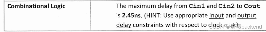
# The maximum delay through the combinational logic is 2.45ns. This can be constrained by pretending that there are
# launching registers on the input ports Cin1 and Cin2 and capturing registers on the output port Cout, and applying
# corresponding input and output delays. The sum of the external input and output delay values must be equal to the
# clock period minus the clock uncertainty minus the maximum combo delay = 3ns - 0.15ns - 2.45ns = 0.4ns.
# This means that the input and output delay values can be 0.4 and 0.0, or 0.2 and 0.2, or 0.1 and 0.3, etc., respectively.
#
set_input_delay -max 0.3 -clock my_clk [get_ports Cin*]
set_output_delay -max 0.1 -clock my_clk [get_ports Cout]

1.5 ENVIRONMENTAL ATTRIBUTES
- clk attribute在设置clock时就指定过了
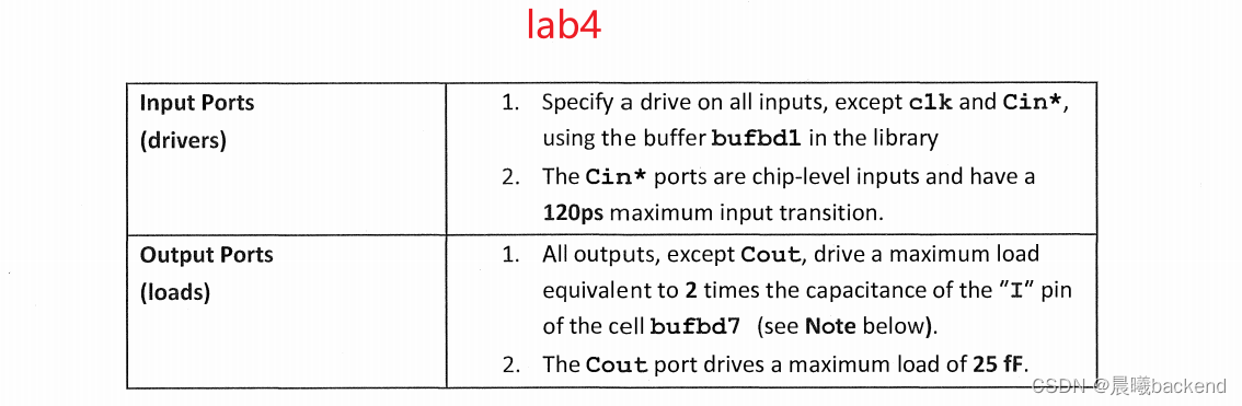
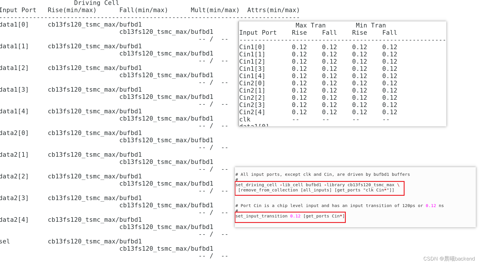
# All input ports, except clk and Cin, are driven by bufbd1 buffers
#
set_driving_cell -lib_cell bufbd1 -library cb13fs120_tsmc_max [remove_from_collection [all_inputs] [get_ports "clk Cin*"]]

# Port Cin is a chip level input and has an input transition of 120ps or 0.12 ns
#
set_input_transition 0.12 [get_ports Cin*]

# All outputs, except Cout, drive 2x bufbd7 loads
#
set_load [expr 2 * {[load_of cb13fs120_tsmc_max/bufbd7/I]}] [get_ports out*]

# Cout drives 25fF, or .025 pF
#
set_load 0.025 [get_ports Cout*]

# operating condition use to scale cell and net delays.
#
set_operating_conditions -max cb13fs120_tsmc_max
2. Addition Constraints Options(在DC LAB4基础上新增的)
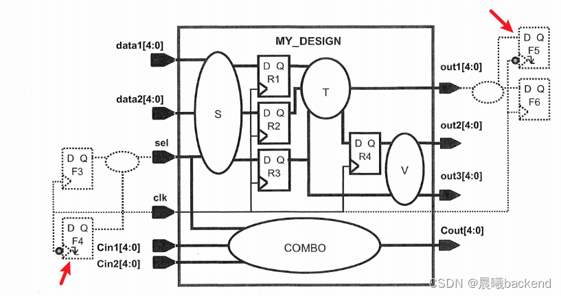
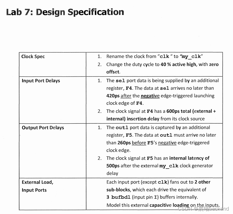
2.1 ADDITIONAL NEG-EDGE INPUT TIMING(F4)

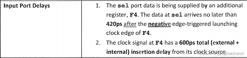
# An additional input delay (-add_delay) of 420ps or 0.42 is applied to the sel port, with respect to a negative edge-triggered
# register F4 (-clock_fall). The total clock insertion delay to F4 is supposed to be 600ps, while the default clock insertion
# delay of 700ps (source) + 300ps (network) = 1000ps is being applied. We can model this by "including" the non-default
# source + network latency total with the input delay value
#
set_input_delay -max  1.02 -clock my_clk -add_delay -clock_fall  -network_latency_included -source_latency_included [get_ports sel]
#input delay 理论约束到0.42ns,但是现在到F4的clk有延迟0.6ns(和default不一样),所以约束到1.02ns
2.2 ADDITIONAL NEG-EDGE OUTPUT TIMING(F5)

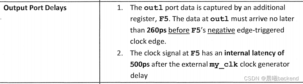
# An additional output delay (-add_delay) of 260ps or 0.26 is applied to the out1 port, with respect to a negative edge-triggered
# register F5 (-clock_fall). To model the 500ps "internal" or network latency, **we must "include" that in the input delay value**.
# We are DELAYING the expected arrival time of the output signal. Since a positive output delay number represents an amount of
# time BEFORE the capturing clock edge, but we want to DELAY the output's capture time, we must SUBTRACT the latency amount from
# the output delay value: Updated output delay = 0.26 - 0.50 = -0.24 !!
#
set_output_delay -max -0.24 -clock my_clk -add_delay -clock_fall -network_latency_included [get_ports out1]

#require time相当于是0.26ns,然后arrival time 相当于 0.5ns,延迟capture time
2.3 EXTERNAL LOAD ON INPUT PORTS

set all_in_ex_clk [remove_from_collection [all_inputs] [get_ports clk]]

# Each input port, except clk, is connected to 2 block, which each drive 3 bufbd1 buffers.
# The capacitive load is therefore 6 bufbd1 buffers, and the fanout is 2. The "fanout"
# is used to calculate more accurate parasitic RC's from the WLM:
#
set_load [expr 6 * {[load_of cb13fs120_tsmc_max/bufbd1/I]}] $all_in_ex_clk
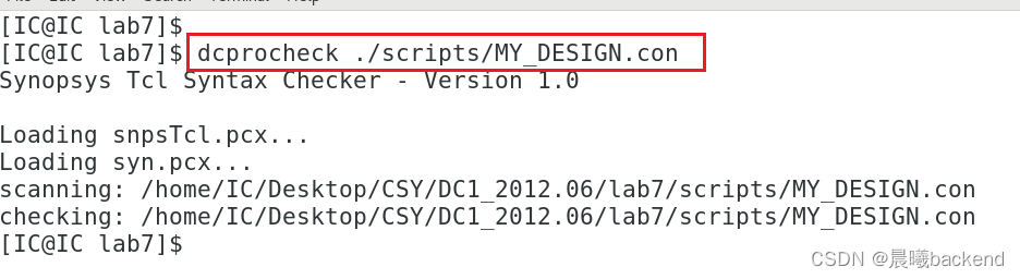
2.4 检查上述约束文件的语法
3. 开始执行DC flow
3.1 启动DC
dc_shell-t -64bit -topo
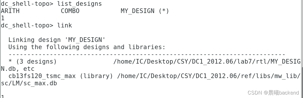
3.2 读入设计、指定顶层、link
read_verilog MY_DESIGN.v
link
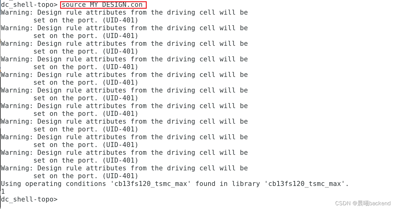
3.3 执行约束文件
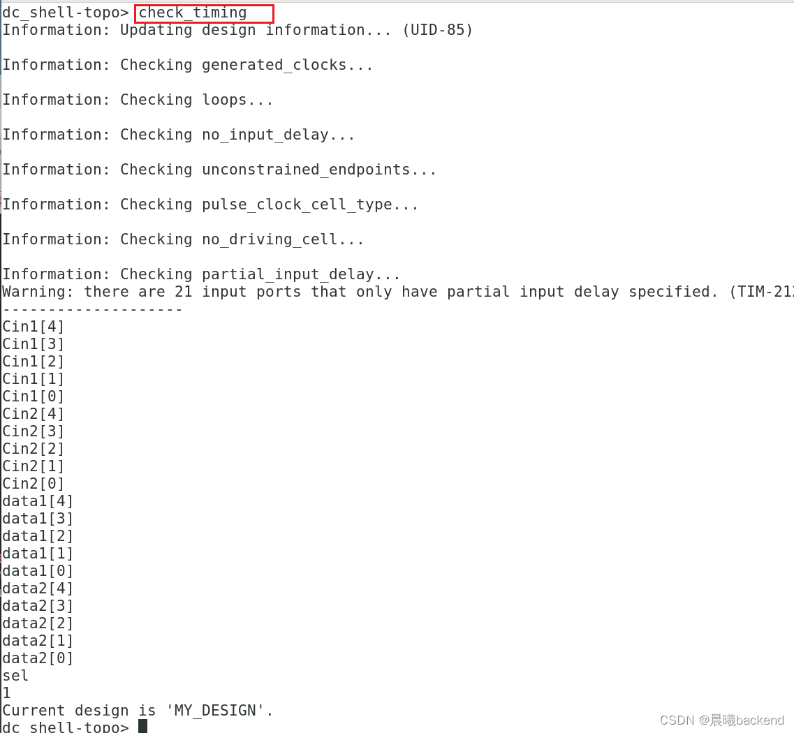
3.4 check_timing(检查有没有没被约束到的)
- warning不用管,setup只需要约束max delay,这里就没有约束min delay
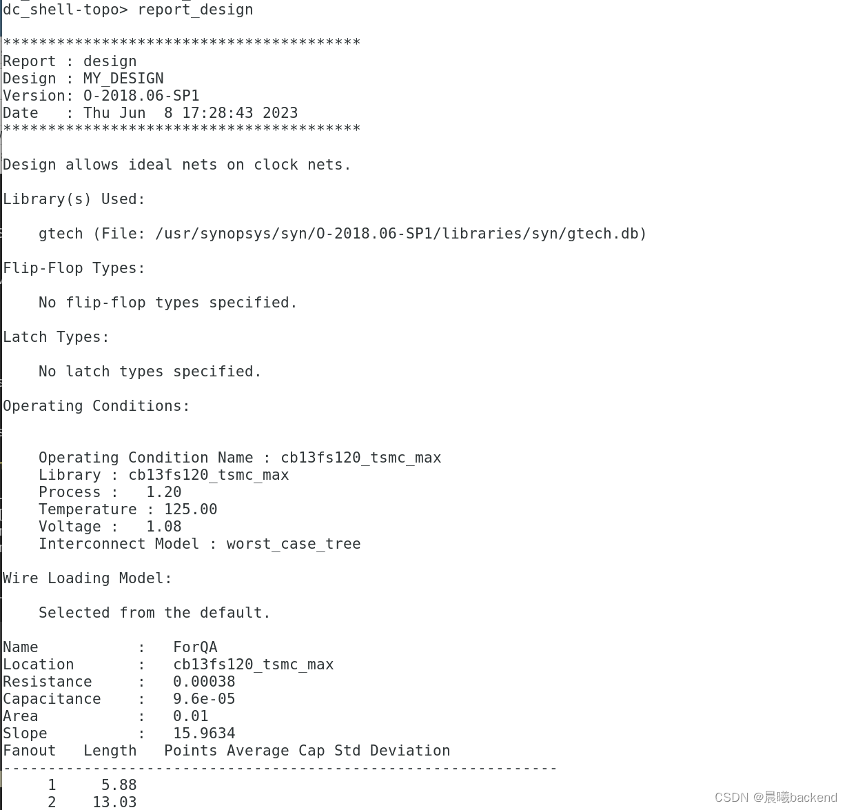
3.5 report_design
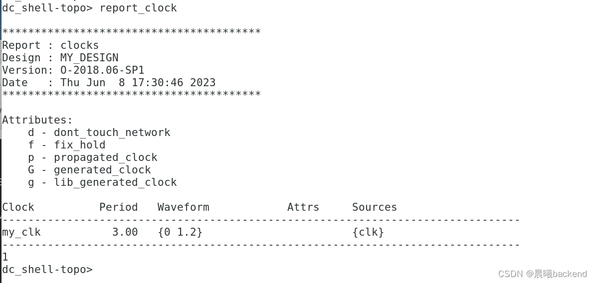
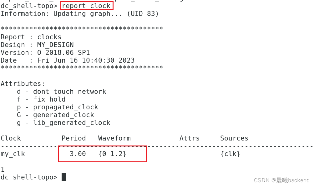
3.6 report_clock
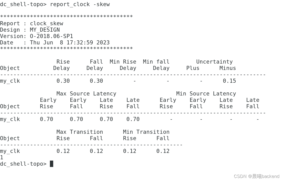
3.7 report_clock -skew
3.8 report_port -verbose
3.8.1 input transition
3.8.2 input delay
3.8.3 output delay
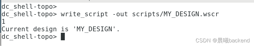
3.9 write_script,将约束文件写出为.wssr
write_script -out scripts/MY_DESIGN.wscr
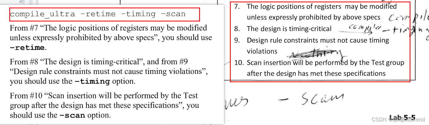
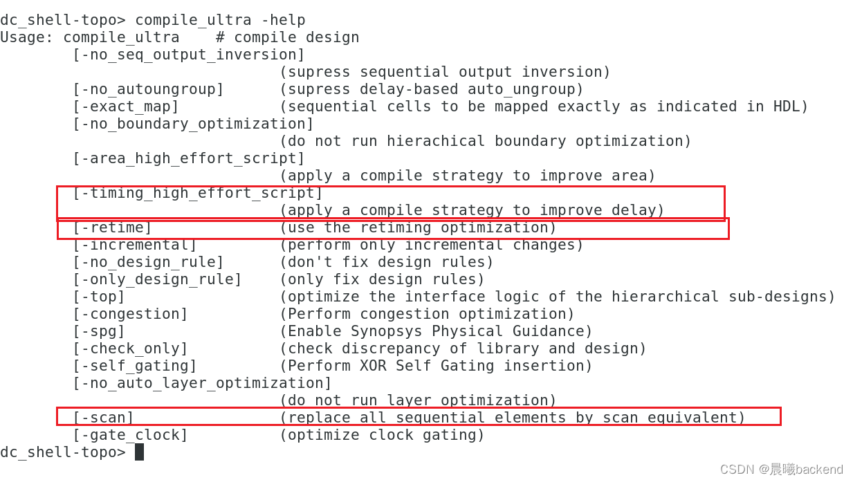
3.10 compile(以下三种都行)
compile_ultra -scan -timing -retime
redirect -tee -file compile.log  {compile_ultra -scan -timing -retime}
redirect -file compile.log  {compile_ultra -scan -timing -retime}

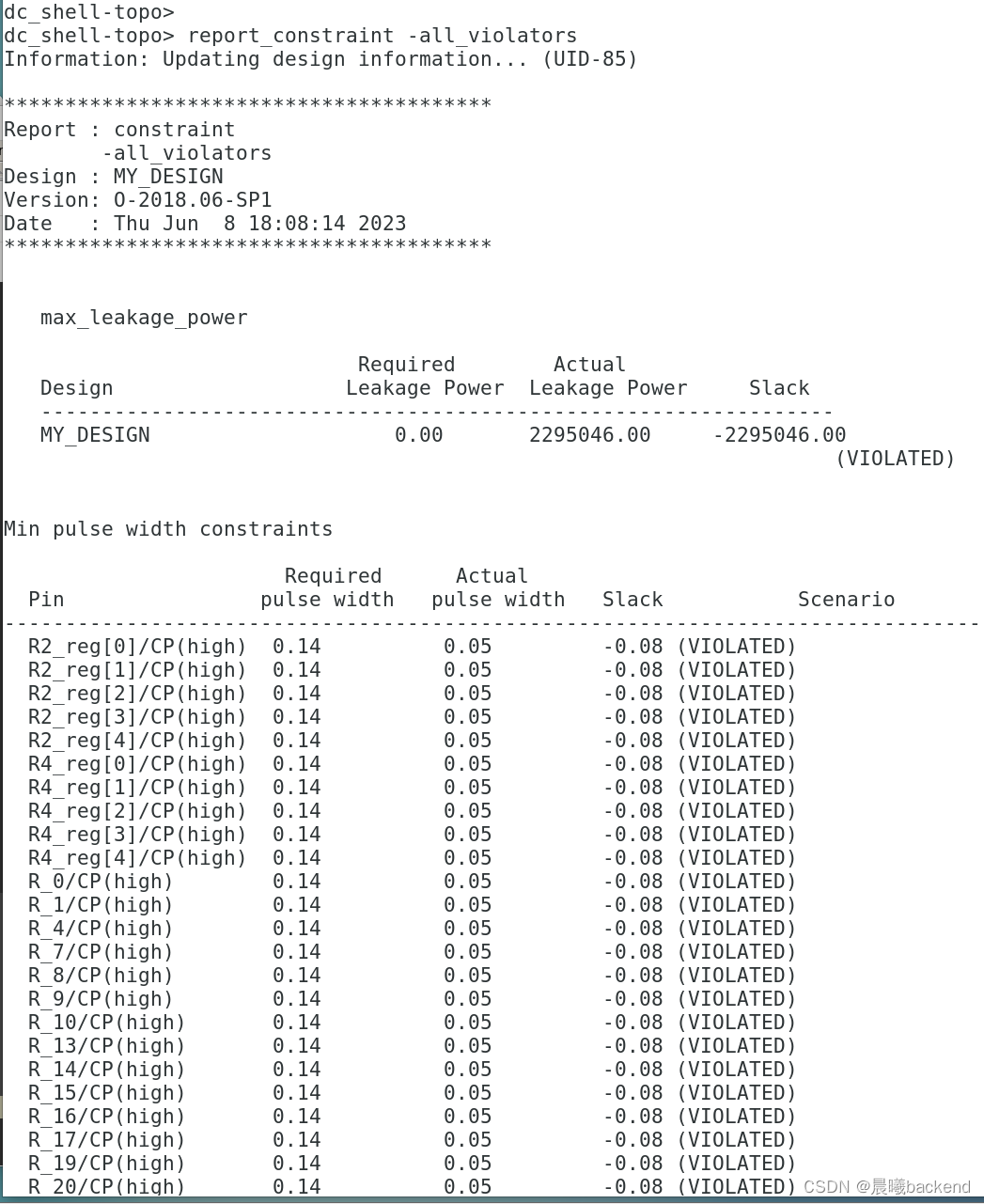
3.11 report_constraint -all_violators
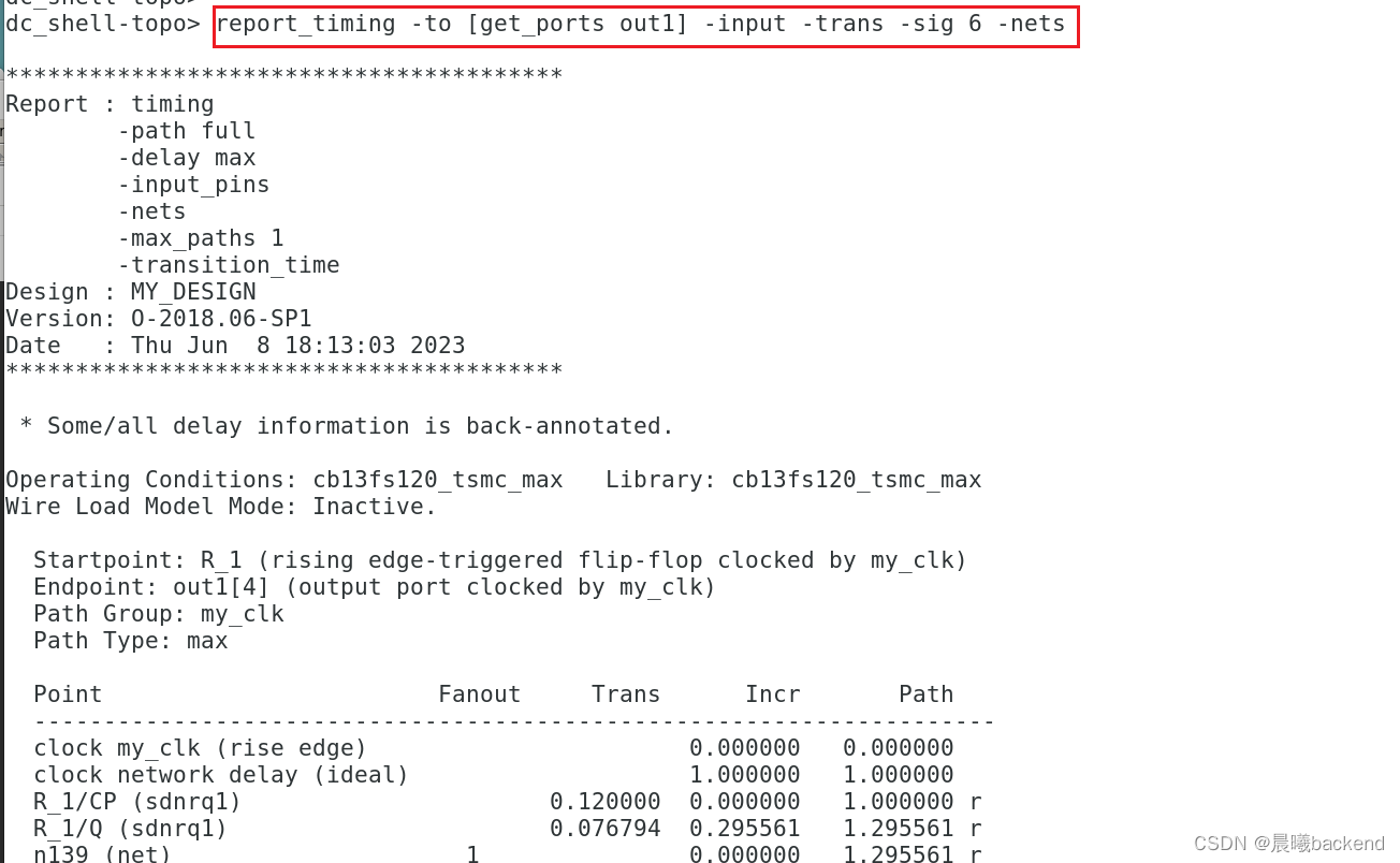
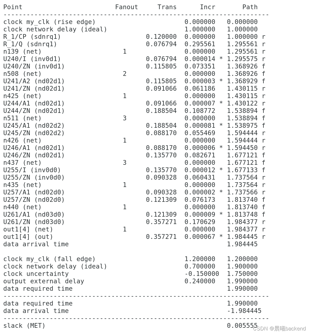
3.12 report_timing -to [get_ports out1] -input -trans -sig 6 -nets
-
Generate a timing report for the path to the out1 output. Include options to show net transition times and net delays to 6 decimal places, as well as net fanout’.
-
注意clk是下降沿触发
*
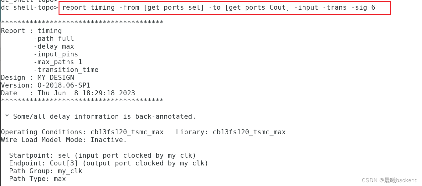
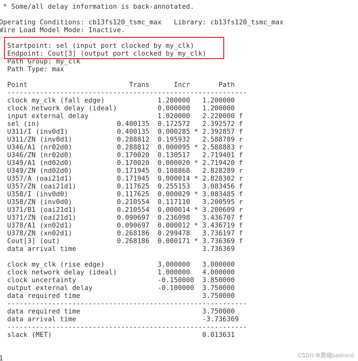
3.13 report_timing -from [get_ports sel] -to [get_ports Cout] -input -trans -sig 6
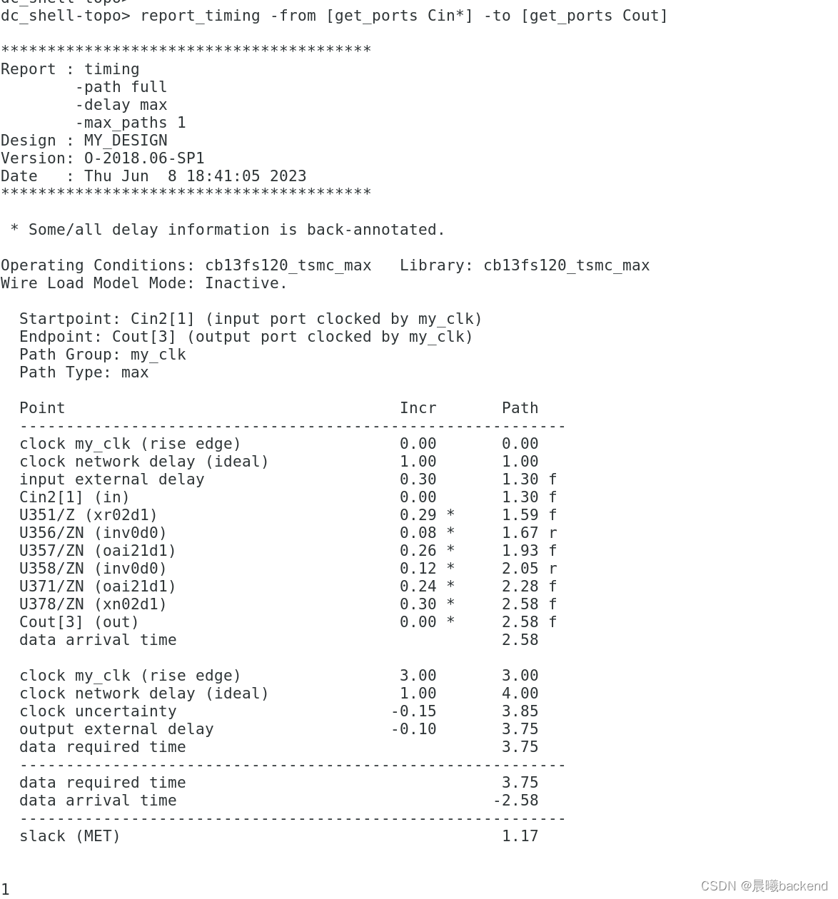
3.14 report_timing -from [get_ports Cin*] -to [get_ports Cout]
3.15 保存设计
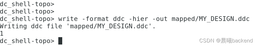
write -format ddc -hier -out mapped/MY_DESIGN.ddc


 1711
1711

 被折叠的 条评论
为什么被折叠?
被折叠的 条评论
为什么被折叠?
 到【灌水乐园】发言


