


 该文详述了设计规划的步骤,包括加载设计、初始化floorplan、预放置与I/Opads相连的宏单元。在初始化floorplan中,创建并定位padcells,设置芯片尺寸和核心区域,插入padfiller以填充间隙。接着,识别并手动放置与I/Opads相连的宏单元,以缩短连接路径。最后,执行虚拟扁平放置,考虑时间和优化策略,以优化布局并减少布线拥堵。
文章目录
Lab 2 Design Planning
2.1 Load the Design
- 进入lab2_dp目录并打开icc_shell,
- 打开orca_lib.mw下的orca_setup cell
- Take a look at the LayoutWindow. 看看跳出的LayoutWindow
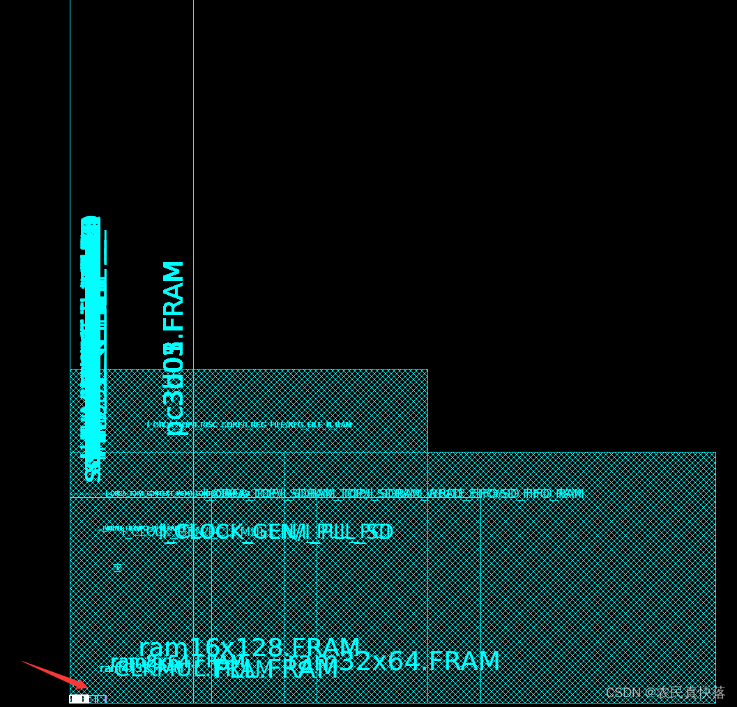
The large greenish-blue rectangles are the macro and IO pad cells, and the small purple rectangles in the lower left corner (zoom in if you want to see them more clearly), are the standard cells.
大的蓝绿色矩形是宏单元格和IO单元格,左下角的紫色小矩形(如果想看得更清楚,可以放大)是标准单元格。
All of these cells are instantiated cells in the netlist.
所有这些单元格都是网络列表中的实例化单元格。
They are all stacked on top of each other at the origin (0,0).
它们都在原点(0,0)处堆叠在一起。
Apply timing and optimization controls which are specified in ./scripts/opt_ctrl.tcl
应用在./scripts/opt_ctrl.tcl中时序和优化控制
# - - - - - - - - - - - - - - - - - - - - - - - - - - - - - - - - - - - - - - -
# General timing and optimization control settings
# - - - - - - - - - - - - - - - - - - - - - - - - - - - - - - - - - - - - - - -
set_app_var timing_enable_multiple_clocks_per_reg true
set_app_var case_analysis_with_logic_constants true
set_app_var physopt_delete_unloaded_cells false
# set physopt_power_critical_range 0.8
# set physopt_area_critical_range 0.8
set_app_var enable_recovery_removal_arcs true

# set_false_path from <clock_name> -to <clock_name>
set_fix_multiple_port_nets -all -buffer_constants
set_auto_disable_drc_nets -constant false
set_timing_derate -max -early 0.95
# set_dont_use <off_limit_cells>
# set_prefer -min <hold_fixing_cells>
set_max_area 0
group_path -name INPUTS -from [all_inputs]
group_path -name OUTPUTS -to [all_outputs]
group_path -name COMBO -from [all_inputs] -to [all_outputs]
set_ideal_network [all_fanout -flat -clock_tree]
# set_cost_priority {max_transistion max_delay}
Most of these settings are discussed in the Appendix of Unit 1. Some are discussed in later Units. Do not spend time here trying to
understand them
这些设置大多数在第一单元的附录中讨论过。其中一些将在后面的单元中讨论。不要在这里花时间试图去理解它们。
2.2 Initialize the Floorplan
- Create physical-only pad cell(PG cell,corner cell), specify pad cell location
- Create floorplan(设置好die size和core area)
- Insert pad filler
- Place macros
- Apply placement blockage
- 添加physical only cells(tap cell, endcap cell, decap cell)
- Build power network
- 对于多电压域设计还要create voltage area等等
The logical netlist from synthesis does not contain physical-only cells such as power and ground pad cells or corner pad cells. You have to therefore create these extra cells before being able to physically place them in the periphery area of your chip.
来自综合的逻辑网表不包含物理单元,如电源和接地单元或角落单元。你需要先创建这些单元,然后才能在芯片的外围区域摆放。
Create the corner and P/G cells and define all pad cell positions using a provided script
创建这些角单元和P/G单元,并使用一个提供的脚本来定义所有pad cell。
Hint:When typing use the [Tab] key for command/option/file completion.
输入时使用Tab键来补全命令/选项/文件
source –echo scripts/pad_cell_cons.tcl
# Create corners and P/G pads
create_cell {

   cornerll cornerlr cornerul cornerur} pfrelr
create_cell {

   vss1left vss1right vss1top vss1bottom} pv0i
create_cell {

   vdd1left vdd1right vdd1top vdd1bottom} pvdi
create_cell {

   vss2left vss2right vss2top vss2bottom} pv0a
create_cell {

   vdd2left vdd2right vdd2top vdd2bottom} pvda

# Define corner pad locations
set_pad_physical_constraints -pad_name "cornerul" -side 1
set_pad_physical_constraints -pad_name "cornerur" -side 2
set_pad_physical_constraints -pad_name "cornerlr" -side 3
set_pad_physical_constraints -pad_name "cornerll" -side 4

# Define signal and PG  pad locations

# Left side
set_pad_physical_constraints -pad_name "pad_iopad_0" -side 1 -order 1
set_pad_physical_constraints -pad_name "pad_iopad_1" -side 1 -order 2
set_pad_physical_constraints -pad_name "pad_iopad_2" -side 1 -order 3
set_pad_physical_constraints -pad_name "pad_iopad_3" -side 1 -order 4
set_pad_physical_constraints -pad_name "pad_iopad_4" -side 1 -order 5
set_pad_physical_constraints -pad_name "pad_iopad_5" -side 1 -order 6
set_pad_physical_constraints -pad_name "pad_iopad_6" -side 1 -order 7
set_pad_physical_constraints -pad_name "pad_iopad_7" -side 1 -order 8
set_pad_physical_constraints -pad_name "pad_iopad_8" -side
最低0.47元/天 解锁文章


 817
817

 被折叠的 条评论
为什么被折叠?
被折叠的 条评论
为什么被折叠?
 到【灌水乐园】发言


