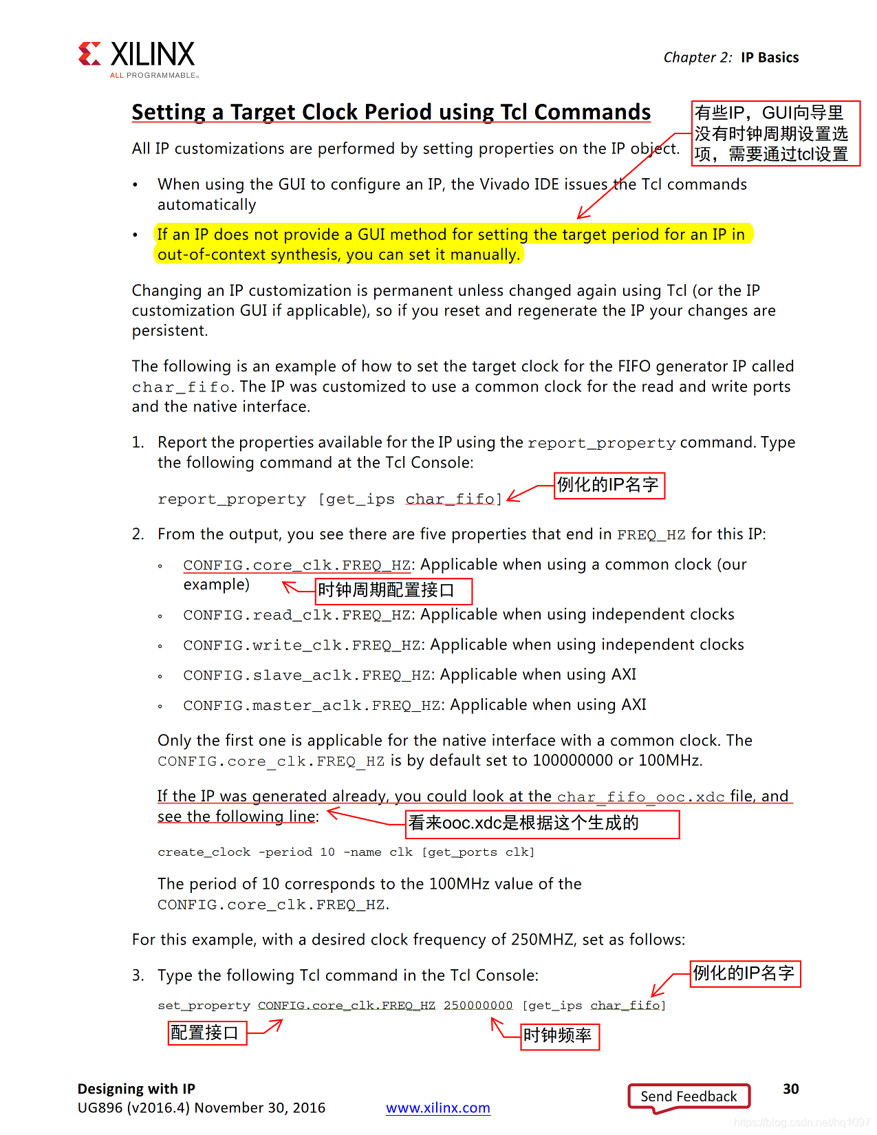
分析CPLD程序编译不通过对原因并解决:Info: *******************************************************************
Info: Running Quartus Prime Analysis & Synthesis
Info: Version 23.1std.1 Build 993 05/14/2024 SC Lite Edition
Info: Processing started: Mon Sep 15 13:40:26 2025
Info: Version 23.1std.1 Build 993 05/14/2024 SC Lite Edition
Info: Processing started: Mon Sep 15 13:40:26 2025
Info: Command: quartus_map --read_settings_files=on --write_settings_files=off i2cfpga -c i2cfpga
Info (16303): High Performance Effort optimization mode selected -- timing performance will be prioritized at the potential cost of increased compilation time
Info (20032): Parallel compilation is enabled and will use up to 4 processors
Info (12021): Found 1 design units, including 1 entities, in source file src/sim/wb_master_model.v
Info (12023): Found entity 1: wb_master_model
Info (12023): Found entity 1: wb_master_model
Info (12021): Found 1 design units, including 1 entities, in source file src/sim/tst_bench_top.v
Info (12023): Found entity 1: tst_bench_top
Info (12023): Found entity 1: tst_bench_top
Info (12021): Found 0 design units, including 0 entities, in source file src/sim/timescale.v
Info (12021): Found 1 design units, including 1 entities, in source file src/sim/i2c_master_top.v
Info (12023): Found entity 1: i2c_master_top
Info (12023): Found entity 1: i2c_master_top
Info (12021): Found 0 design units, including 0 entities, in source file src/sim/i2c_master_defines.v
Info (12021): Found 1 design units, including 1 entities, in source file src/sim/i2c_master_byte_ctrl.v
Info (12023): Found entity 1: i2c_master_byte_ctrl
Info (12023): Found entity 1: i2c_master_byte_ctrl
Info (12021): Found 1 design units, including 1 entities, in source file src/sim/i2c_master_bit_ctrl.v
Info (12023): Found entity 1: i2c_master_bit_ctrl
Info (12023): Found entity 1: i2c_master_bit_ctrl
Info (15248): File "C:/Users/YG/Desktop/i2ccpld_20250729/i2ccpld_20250729/i2cfpga0421_restored/src/timescale.v" is a duplicate of already analyzed file "C:/Users/YG/Desktop/i2ccpld_20250729/i2ccpld_20250729/i2cfpga0421_restored/src/sim/timescale.v" (same filename, same library name and same md5 digest). Skipping analysis of this file.
Info (12021): Found 0 design units, including 0 entities, in source file src/timescale.v
Info (12021): Found 1 design units, including 1 entities, in source file src/myram.v
Info (12023): Found entity 1: myRAM
Info (12023): Found entity 1: myRAM
Info (12021): Found 1 design units, including 1 entities, in source file src/i2cslave.v
Info (12023): Found entity 1: I2Cslave
Info (12023): Found entity 1: I2Cslave
Info (15248): File "C:/Users/YG/Desktop/i2ccpld_20250729/i2ccpld_20250729/i2cfpga0421_restored/timescale.v" is a duplicate of already analyzed file "C:/Users/YG/Desktop/i2ccpld_20250729/i2ccpld_20250729/i2cfpga0421_restored/src/sim/timescale.v" (same filename, same library name and same md5 digest). Skipping analysis of this file.
Info (12021): Found 0 design units, including 0 entities, in source file timescale.v
Info (12021): Found 1 design units, including 1 entities, in source file pulse_reg_top.v
Info (12023): Found entity 1: pulse_reg_top
Info (12023): Found entity 1: pulse_reg_top
Info (12021): Found 1 design units, including 1 entities, in source file pulse_reg_gen4.v
Info (12023): Found entity 1: pulse_reg_gen4
Info (12023): Found entity 1: pulse_reg_gen4
Info (12021): Found 1 design units, including 1 entities, in source file pulse_reg.v
Info (12023): Found entity 1: pulse_reg
Info (12023): Found entity 1: pulse_reg
Info (12021): Found 1 design units, including 1 entities, in source file pll4x.v
Info (12023): Found entity 1: pll4x
Info (12023): Found entity 1: pll4x
Info (12127): Elaborating entity "pulse_reg_top" for the top level hierarchy
Info (12128): Elaborating entity "I2Cslave" for hierarchy "I2Cslave:I2Cslave_inst"
Info (12128): Elaborating entity "pulse_reg" for hierarchy "pulse_reg:pulse_reg_inst"
Info (12128): Elaborating entity "pulse_reg_gen4" for hierarchy "pulse_reg_gen4:pulse_reg_gen4_inst"
Info (12128): Elaborating entity "pll4x" for hierarchy "pulse_reg_gen4:pulse_reg_gen4_inst|pll4x:pll4x"
Info (12128): Elaborating entity "altpll" for hierarchy "pulse_reg_gen4:pulse_reg_gen4_inst|pll4x:pll4x|altpll:altpll_component"
Info (12130): Elaborated megafunction instantiation "pulse_reg_gen4:pulse_reg_gen4_inst|pll4x:pll4x|altpll:altpll_component"
Info (12133): Instantiated megafunction "pulse_reg_gen4:pulse_reg_gen4_inst|pll4x:pll4x|altpll:altpll_component" with the following parameter:
Info (12134): Parameter "bandwidth_type" = "AUTO"
Info (12134): Parameter "clk0_divide_by" = "1"
Info (12134): Parameter "clk0_duty_cycle" = "50"
Info (12134): Parameter "clk0_multiply_by" = "4"
Info (12134): Parameter "clk0_phase_shift" = "0"
Info (12134): Parameter "clk1_divide_by" = "1"
Info (12134): Parameter "clk1_duty_cycle" = "50"
Info (12134): Parameter "clk1_multiply_by" = "4"
Info (12134): Parameter "clk1_phase_shift" = "2500"
Info (12134): Parameter "compensate_clock" = "CLK0"
Info (12134): Parameter "inclk0_input_frequency" = "20000"
Info (12134): Parameter "intended_device_family" = "Cyclone IV E"
Info (12134): Parameter "lpm_hint" = "CBX_MODULE_PREFIX=pll4x"
Info (12134): Parameter "lpm_type" = "altpll"
Info (12134): Parameter "operation_mode" = "NORMAL"
Info (12134): Parameter "pll_type" = "AUTO"
Info (12134): Parameter "port_activeclock" = "PORT_UNUSED"
Info (12134): Parameter "port_areset" = "PORT_UNUSED"
Info (12134): Parameter "port_clkbad0" = "PORT_UNUSED"
Info (12134): Parameter "port_clkbad1" = "PORT_UNUSED"
Info (12134): Parameter "port_clkloss" = "PORT_UNUSED"
Info (12134): Parameter "port_clkswitch" = "PORT_UNUSED"
Info (12134): Parameter "port_configupdate" = "PORT_UNUSED"
Info (12134): Parameter "port_fbin" = "PORT_UNUSED"
Info (12134): Parameter "port_inclk0" = "PORT_USED"
Info (12134): Parameter "port_inclk1" = "PORT_UNUSED"
Info (12134): Parameter "port_locked" = "PORT_USED"
Info (12134): Parameter "port_pfdena" = "PORT_UNUSED"
Info (12134): Parameter "port_phasecounterselect" = "PORT_UNUSED"
Info (12134): Parameter "port_phasedone" = "PORT_UNUSED"
Info (12134): Parameter "port_phasestep" = "PORT_UNUSED"
Info (12134): Parameter "port_phaseupdown" = "PORT_UNUSED"
Info (12134): Parameter "port_pllena" = "PORT_UNUSED"
Info (12134): Parameter "port_scanaclr" = "PORT_UNUSED"
Info (12134): Parameter "port_scanclk" = "PORT_UNUSED"
Info (12134): Parameter "port_scanclkena" = "PORT_UNUSED"
Info (12134): Parameter "port_scandata" = "PORT_UNUSED"
Info (12134): Parameter "port_scandataout" = "PORT_UNUSED"
Info (12134): Parameter "port_scandone" = "PORT_UNUSED"
Info (12134): Parameter "port_scanread" = "PORT_UNUSED"
Info (12134): Parameter "port_scanwrite" = "PORT_UNUSED"
Info (12134): Parameter "port_clk0" = "PORT_USED"
Info (12134): Parameter "port_clk1" = "PORT_USED"
Info (12134): Parameter "port_clk2" = "PORT_UNUSED"
Info (12134): Parameter "port_clk3" = "PORT_UNUSED"
Info (12134): Parameter "port_clk4" = "PORT_UNUSED"
Info (12134): Parameter "port_clk5" = "PORT_UNUSED"
Info (12134): Parameter "port_clkena0" = "PORT_UNUSED"
Info (12134): Parameter "port_clkena1" = "PORT_UNUSED"
Info (12134): Parameter "port_clkena2" = "PORT_UNUSED"
Info (12134): Parameter "port_clkena3" = "PORT_UNUSED"
Info (12134): Parameter "port_clkena4" = "PORT_UNUSED"
Info (12134): Parameter "port_clkena5" = "PORT_UNUSED"
Info (12134): Parameter "port_extclk0" = "PORT_UNUSED"
Info (12134): Parameter "port_extclk1" = "PORT_UNUSED"
Info (12134): Parameter "port_extclk2" = "PORT_UNUSED"
Info (12134): Parameter "port_extclk3" = "PORT_UNUSED"
Info (12134): Parameter "self_reset_on_loss_lock" = "OFF"
Info (12134): Parameter "width_clock" = "5"
Info (12021): Found 1 design units, including 1 entities, in source file db/pll4x_altpll.v
Info (12023): Found entity 1: pll4x_altpll
Info (12023): Found entity 1: pll4x_altpll
Info (12128): Elaborating entity "pll4x_altpll" for hierarchy "pulse_reg_gen4:pulse_reg_gen4_inst|pll4x:pll4x|altpll:altpll_component|pll4x_altpll:auto_generated"
Info (13000): Registers with preset signals will power-up high
Info (13003): DEV_CLRn pin will set, and not reset, register with preset signal due to NOT Gate Push-Back
Info (286030): Timing-Driven Synthesis is running
Info (17049): 3 registers lost all their fanouts during netlist optimizations.
Info (128000): Starting physical synthesis optimizations for speed
Info (332104): Reading SDC File: 'I2Cslave.sdc'
Info (332110): Deriving PLL clocks
Info (332110): create_generated_clock -source {pulse_reg_gen4_inst|pll4x|altpll_component|auto_generated|pll1|inclk[0]} -multiply_by 4 -duty_cycle 50.00 -name {pulse_reg_gen4_inst|pll4x|altpll_component|auto_generated|pll1|clk[0]} {pulse_reg_gen4_inst|pll4x|altpll_component|auto_generated|pll1|clk[0]}
Info (332110): create_generated_clock -source {pulse_reg_gen4_inst|pll4x|altpll_component|auto_generated|pll1|inclk[0]} -multiply_by 4 -phase 180.00 -duty_cycle 50.00 -name {pulse_reg_gen4_inst|pll4x|altpll_component|auto_generated|pll1|clk[1]} {pulse_reg_gen4_inst|pll4x|altpll_component|auto_generated|pll1|clk[1]}
Info (332151): Clock uncertainty is not calculated until you update the timing netlist.
Info (332154): The derive_clock_uncertainty command did not apply clock uncertainty to any clock-to-clock transfers.
Info (332129): Detected timing requirements -- optimizing circuit to achieve only the specified requirements
Info (332111): Found 3 clocks
Info (332111): Period Clock Name
Info (332111): ======== ============
Info (332111): 20.000 clk
Info (332111): 5.000 pulse_reg_gen4_inst|pll4x|altpll_component|auto_generated|pll1|clk[0]
Info (332111): 5.000 pulse_reg_gen4_inst|pll4x|altpll_component|auto_generated|pll1|clk[1]
Info (332111): Period Clock Name
Info (332111): ======== ============
Info (332111): 20.000 clk
Info (332111): 5.000 pulse_reg_gen4_inst|pll4x|altpll_component|auto_generated|pll1|clk[0]
Info (332111): 5.000 pulse_reg_gen4_inst|pll4x|altpll_component|auto_generated|pll1|clk[1]
Info (128002): Starting physical synthesis algorithm register retiming
Info (128003): Physical synthesis algorithm register retiming complete: estimated slack improvement of 1243 ps
Info (128002): Starting physical synthesis algorithm combinational resynthesis using boolean division
Info (128003): Physical synthesis algorithm combinational resynthesis using boolean division complete: estimated slack improvement of 0 ps
Info (128001): Physical synthesis optimizations for speed complete: elapsed time is 00:00:01
Info (144001): Generated suppressed messages file C:/Users/YG/Desktop/i2ccpld_20250729/i2ccpld_20250729/i2cfpga0421_restored/output_files/i2cfpga.map.smsg
Info (16010): Generating hard_block partition "hard_block:auto_generated_inst"
Info (16011): Adding 1 node(s), including 0 DDIO, 1 PLL, 0 transceiver and 0 LCELL
Info (16011): Adding 1 node(s), including 0 DDIO, 1 PLL, 0 transceiver and 0 LCELL
Info (21057): Implemented 1035 device resources after synthesis - the final resource count might be different
Info (21058): Implemented 5 input pins
Info (21059): Implemented 11 output pins
Info (21060): Implemented 1 bidirectional pins
Info (21061): Implemented 1017 logic cells
Info (21065): Implemented 1 PLLs
Info (21058): Implemented 5 input pins
Info (21059): Implemented 11 output pins
Info (21060): Implemented 1 bidirectional pins
Info (21061): Implemented 1017 logic cells
Info (21065): Implemented 1 PLLs
Info: Quartus Prime Analysis & Synthesis was successful. 0 errors, 0 warnings
Info: Peak virtual memory: 4846 megabytes
Info: Processing ended: Mon Sep 15 13:40:36 2025
Info: Elapsed time: 00:00:10
Info: Total CPU time (on all processors): 00:00:09
Info: Peak virtual memory: 4846 megabytes
Info: Processing ended: Mon Sep 15 13:40:36 2025
Info: Elapsed time: 00:00:10
Info: Total CPU time (on all processors): 00:00:09
Info: *******************************************************************
Info: Running Quartus Prime Fitter
Info: Version 23.1std.1 Build 993 05/14/2024 SC Lite Edition
Info: Processing started: Mon Sep 15 13:40:37 2025
Info: Version 23.1std.1 Build 993 05/14/2024 SC Lite Edition
Info: Processing started: Mon Sep 15 13:40:37 2025
Info: Command: quartus_fit --read_settings_files=off --write_settings_files=off i2cfpga -c i2cfpga
Info: qfit2_default_script.tcl version: #1
Info: Project = i2cfpga
Info: Revision = i2cfpga
Info (16303): High Performance Effort optimization mode selected -- timing performance will be prioritized at the potential cost of increased compilation time
Info (20032): Parallel compilation is enabled and will use up to 4 processors
Info (119006): Selected device EP4CE6F17C8 for design "i2cfpga"
Info (21077): Low junction temperature is 0 degrees C
Info (21077): High junction temperature is 85 degrees C
Info (15535): Implemented PLL "pulse_reg_gen4:pulse_reg_gen4_inst|pll4x:pll4x|altpll:altpll_component|pll4x_altpll:auto_generated|pll1" as Cyclone IV E PLL type
Info (15099): Implementing clock multiplication of 4, clock division of 1, and phase shift of 0 degrees (0 ps) for pulse_reg_gen4:pulse_reg_gen4_inst|pll4x:pll4x|altpll:altpll_component|pll4x_altpll:auto_generated|wire_pll1_clk[0] port
Info (15099): Implementing clock multiplication of 4, clock division of 1, and phase shift of 180 degrees (2500 ps) for pulse_reg_gen4:pulse_reg_gen4_inst|pll4x:pll4x|altpll:altpll_component|pll4x_altpll:auto_generated|wire_pll1_clk[1] port
Info (171004): Fitter is performing a Standard Fit compilation using maximum Fitter effort to optimize design performance
Warning (292013): Feature LogicLock is only available with a valid subscription license. You can purchase a software subscription to gain full access to this feature.
Info (176444): Device migration not selected. If you intend to use device migration later, you may need to change the pin assignments as they may be incompatible with other devices
Info (176445): Device EP4CE10F17C8 is compatible
Info (176445): Device EP4CE15F17C8 is compatible
Info (176445): Device EP4CE22F17C8 is compatible
Info (176445): Device EP4CE10F17C8 is compatible
Info (176445): Device EP4CE15F17C8 is compatible
Info (176445): Device EP4CE22F17C8 is compatible
Info (169124): Fitter converted 5 user pins into dedicated programming pins
Info (169125): Pin ~ALTERA_ASDO_DATA1~ is reserved at location C1
Info (169125): Pin ~ALTERA_FLASH_nCE_nCSO~ is reserved at location D2
Info (169125): Pin ~ALTERA_DCLK~ is reserved at location H1
Info (169125): Pin ~ALTERA_DATA0~ is reserved at location H2
Info (169125): Pin ~ALTERA_nCEO~ is reserved at location F16
Info (332104): Reading SDC File: 'I2Cslave.sdc'
Info (332110): Deriving PLL clocks
Info (332110): create_generated_clock -source {pulse_reg_gen4_inst|pll4x|altpll_component|auto_generated|pll1|inclk[0]} -multiply_by 4 -duty_cycle 50.00 -name {pulse_reg_gen4_inst|pll4x|altpll_component|auto_generated|pll1|clk[0]} {pulse_reg_gen4_inst|pll4x|altpll_component|auto_generated|pll1|clk[0]}
Info (332110): create_generated_clock -source {pulse_reg_gen4_inst|pll4x|altpll_component|auto_generated|pll1|inclk[0]} -multiply_by 4 -phase 180.00 -duty_cycle 50.00 -name {pulse_reg_gen4_inst|pll4x|altpll_component|auto_generated|pll1|clk[1]} {pulse_reg_gen4_inst|pll4x|altpll_component|auto_generated|pll1|clk[1]}
Info (332110): create_generated_clock -source {pulse_reg_gen4_inst|pll4x|altpll_component|auto_generated|pll1|inclk[0]} -multiply_by 4 -duty_cycle 50.00 -name {pulse_reg_gen4_inst|pll4x|altpll_component|auto_generated|pll1|clk[0]} {pulse_reg_gen4_inst|pll4x|altpll_component|auto_generated|pll1|clk[0]}
Info (332110): create_generated_clock -source {pulse_reg_gen4_inst|pll4x|altpll_component|auto_generated|pll1|inclk[0]} -multiply_by 4 -phase 180.00 -duty_cycle 50.00 -name {pulse_reg_gen4_inst|pll4x|altpll_component|auto_generated|pll1|clk[1]} {pulse_reg_gen4_inst|pll4x|altpll_component|auto_generated|pll1|clk[1]}
Info (332151): Clock uncertainty is not calculated until you update the timing netlist.
Info (332154): The derive_clock_uncertainty command did not apply clock uncertainty to any clock-to-clock transfers.
Info (332129): Detected timing requirements -- optimizing circuit to achieve only the specified requirements
Info (332111): Found 3 clocks
Info (332111): Period Clock Name
Info (332111): ======== ============
Info (332111): 20.000 clk
Info (332111): 5.000 pulse_reg_gen4_inst|pll4x|altpll_component|auto_generated|pll1|clk[0]
Info (332111): 5.000 pulse_reg_gen4_inst|pll4x|altpll_component|auto_generated|pll1|clk[1]
Info (332111): Period Clock Name
Info (332111): ======== ============
Info (332111): 20.000 clk
Info (332111): 5.000 pulse_reg_gen4_inst|pll4x|altpll_component|auto_generated|pll1|clk[0]
Info (332111): 5.000 pulse_reg_gen4_inst|pll4x|altpll_component|auto_generated|pll1|clk[1]
Info (176353): Automatically promoted node clk~input (placed in PIN E1 (CLK1, DIFFCLK_0n))
Info (176355): Automatically promoted destinations to use location or clock signal Global Clock CLKCTRL_G2
Info (176355): Automatically promoted destinations to use location or clock signal Global Clock CLKCTRL_G2
Info (176353): Automatically promoted node pulse_reg_gen4:pulse_reg_gen4_inst|pll4x:pll4x|altpll:altpll_component|pll4x_altpll:auto_generated|wire_pll1_clk[0] (placed in counter C0 of PLL_1)
Info (176355): Automatically promoted destinations to use location or clock signal Global Clock CLKCTRL_G3
Info (176355): Automatically promoted destinations to use location or clock signal Global Clock CLKCTRL_G3
Info (176353): Automatically promoted node pulse_reg_gen4:pulse_reg_gen4_inst|pll4x:pll4x|altpll:altpll_component|pll4x_altpll:auto_generated|wire_pll1_clk[1] (placed in counter C1 of PLL_1)
Info (176355): Automatically promoted destinations to use location or clock signal Global Clock CLKCTRL_G4
Info (176355): Automatically promoted destinations to use location or clock signal Global Clock CLKCTRL_G4
Info (176353): Automatically promoted node comb~0
Info (176355): Automatically promoted destinations to use location or clock signal Global Clock
Info (176356): Following destination nodes may be non-global or may not use global or regional clocks
Info (176357): Destination node I2Cslave:I2Cslave_inst|sda_oe~1
Info (176357): Destination node I2Cslave:I2Cslave_inst|mem_do~2
Info (176357): Destination node I2Cslave:I2Cslave_inst|mem_update~1
Info (176357): Destination node I2Cslave:I2Cslave_inst|bit_cnt~0
Info (176357): Destination node I2Cslave:I2Cslave_inst|bit_cnt[0]~1
Info (176357): Destination node I2Cslave:I2Cslave_inst|ld~0
Info (176357): Destination node I2Cslave:I2Cslave_inst|bit_cnt~3
Info (176357): Destination node I2Cslave:I2Cslave_inst|mem_do~4
Info (176357): Destination node pulse_reg:pulse_reg_inst|out[7]~0
Info (176357): Destination node I2Cslave:I2Cslave_inst|mem_do~5
Info (176358): Non-global destination nodes limited to 10 nodes
Info (176233): Starting register packing
Info (176235): Finished register packing
Extra Info (176219): No registers were packed into other blocks
Extra Info (176219): No registers were packed into other blocks
Info (128000): Starting physical synthesis optimizations for speed
Info (128001): Physical synthesis optimizations for speed complete: elapsed time is 00:00:00
Info (171121): Fitter preparation operations ending: elapsed time is 00:00:02
Info (14896): Fitter has disabled Advanced Physical Optimization because it is not supported for the current family.
Info (170189): Fitter placement preparation operations beginning
Info (170190): Fitter placement preparation operations ending: elapsed time is 00:00:00
Info (170191): Fitter placement operations beginning
Info (170137): Fitter placement was successful
Info (170192): Fitter placement operations ending: elapsed time is 00:00:02
Info (170193): Fitter routing operations beginning
Info (170195): Router estimated average interconnect usage is 1% of the available device resources
Info (170196): Router estimated peak interconnect usage is 8% of the available device resources in the region that extends from location X0_Y0 to location X10_Y11
Info (170196): Router estimated peak interconnect usage is 8% of the available device resources in the region that extends from location X0_Y0 to location X10_Y11
Info (170194): Fitter routing operations ending: elapsed time is 00:00:02
Info (11888): Total time spent on timing analysis during the Fitter is 0.62 seconds.
Info (334003): Started post-fitting delay annotation
Info (334004): Delay annotation completed successfully
Info (334003): Started post-fitting delay annotation
Info (334004): Delay annotation completed successfully
Info (11218): Fitter post-fit operations ending: elapsed time is 00:00:01
Warning (169177): 6 pins must meet Intel FPGA requirements for 3.3-, 3.0-, and 2.5-V interfaces. For more information, refer to AN 447: Interfacing Cyclone IV E Devices with 3.3/3.0/2.5-V LVTTL/LVCMOS I/O Systems.
Info (169178): Pin sda uses I/O standard 3.3-V LVTTL at B6
Info (169178): Pin clk uses I/O standard 3.3-V LVTTL at E1
Info (169178): Pin start_gpio uses I/O standard 3.3-V LVTTL at A5
Info (169178): Pin gpio_rstn uses I/O standard 3.3-V LVTTL at B7
Info (169178): Pin scl uses I/O standard 3.3-V LVTTL at B5
Info (169178): Pin k2 uses I/O standard 3.3-V LVTTL at C16
Info (144001): Generated suppressed messages file C:/Users/YG/Desktop/i2ccpld_20250729/i2ccpld_20250729/i2cfpga0421_restored/output_files/i2cfpga.fit.smsg
Info: Quartus Prime Fitter was successful. 0 errors, 2 warnings
Info: Peak virtual memory: 5497 megabytes
Info: Processing ended: Mon Sep 15 13:40:45 2025
Info: Elapsed time: 00:00:08
Info: Total CPU time (on all processors): 00:00:04
Info: Peak virtual memory: 5497 megabytes
Info: Processing ended: Mon Sep 15 13:40:45 2025
Info: Elapsed time: 00:00:08
Info: Total CPU time (on all processors): 00:00:04
Info: *******************************************************************
Info: Running Quartus Prime Assembler
Info: Version 23.1std.1 Build 993 05/14/2024 SC Lite Edition
Info: Processing started: Mon Sep 15 13:40:46 2025
Info: Version 23.1std.1 Build 993 05/14/2024 SC Lite Edition
Info: Processing started: Mon Sep 15 13:40:46 2025
Info: Command: quartus_asm --read_settings_files=off --write_settings_files=off i2cfpga -c i2cfpga
Info (115031): Writing out detailed assembly data for power analysis
Info (115030): Assembler is generating device programming files
Info: Quartus Prime Assembler was successful. 0 errors, 0 warnings
Info: Peak virtual memory: 4697 megabytes
Info: Processing ended: Mon Sep 15 13:40:47 2025
Info: Elapsed time: 00:00:01
Info: Total CPU time (on all processors): 00:00:00
Info: Peak virtual memory: 4697 megabytes
Info: Processing ended: Mon Sep 15 13:40:47 2025
Info: Elapsed time: 00:00:01
Info: Total CPU time (on all processors): 00:00:00
Info (293026): Skipped module Power Analyzer due to the assignment FLOW_ENABLE_POWER_ANALYZER
Info: *******************************************************************
Info: Running Quartus Prime Timing Analyzer
Info: Version 23.1std.1 Build 993 05/14/2024 SC Lite Edition
Info: Processing started: Mon Sep 15 13:40:48 2025
Info: Version 23.1std.1 Build 993 05/14/2024 SC Lite Edition
Info: Processing started: Mon Sep 15 13:40:48 2025
Info: Command: quartus_sta i2cfpga -c i2cfpga
Info: qsta_default_script.tcl version: #1
Info (20032): Parallel compilation is enabled and will use up to 4 processors
Info (21077): Low junction temperature is 0 degrees C
Info (21077): High junction temperature is 85 degrees C
Info (332104): Reading SDC File: 'I2Cslave.sdc'
Info (332110): Deriving PLL clocks
Info (332110): create_generated_clock -source {pulse_reg_gen4_inst|pll4x|altpll_component|auto_generated|pll1|inclk[0]} -multiply_by 4 -duty_cycle 50.00 -name {pulse_reg_gen4_inst|pll4x|altpll_component|auto_generated|pll1|clk[0]} {pulse_reg_gen4_inst|pll4x|altpll_component|auto_generated|pll1|clk[0]}
Info (332110): create_generated_clock -source {pulse_reg_gen4_inst|pll4x|altpll_component|auto_generated|pll1|inclk[0]} -multiply_by 4 -phase 180.00 -duty_cycle 50.00 -name {pulse_reg_gen4_inst|pll4x|altpll_component|auto_generated|pll1|clk[1]} {pulse_reg_gen4_inst|pll4x|altpll_component|auto_generated|pll1|clk[1]}
Info (332110): create_generated_clock -source {pulse_reg_gen4_inst|pll4x|altpll_component|auto_generated|pll1|inclk[0]} -multiply_by 4 -duty_cycle 50.00 -name {pulse_reg_gen4_inst|pll4x|altpll_component|auto_generated|pll1|clk[0]} {pulse_reg_gen4_inst|pll4x|altpll_component|auto_generated|pll1|clk[0]}
Info (332110): create_generated_clock -source {pulse_reg_gen4_inst|pll4x|altpll_component|auto_generated|pll1|inclk[0]} -multiply_by 4 -phase 180.00 -duty_cycle 50.00 -name {pulse_reg_gen4_inst|pll4x|altpll_component|auto_generated|pll1|clk[1]} {pulse_reg_gen4_inst|pll4x|altpll_component|auto_generated|pll1|clk[1]}
Info (332151): Clock uncertainty is not calculated until you update the timing netlist.
Info (332123): Deriving Clock Uncertainty. Please refer to report_sdc in the Timing Analyzer to see clock uncertainties.
Info: Found TIMING_ANALYZER_REPORT_SCRIPT_INCLUDE_DEFAULT_ANALYSIS = ON
Info: Analyzing Slow 1200mV 85C Model
Info (332146): Worst-case setup slack is 0.075
Info (332119): Slack End Point TNS Clock
Info (332119): ========= =================== =====================
Info (332119): 0.075 0.000 pulse_reg_gen4_inst|pll4x|altpll_component|auto_generated|pll1|clk[0]
Info (332119): 0.143 0.000 pulse_reg_gen4_inst|pll4x|altpll_component|auto_generated|pll1|clk[1]
Info (332119): 13.520 0.000 clk
Info (332146): Worst-case hold slack is 0.432
Info (332119): Slack End Point TNS Clock
Info (332119): ========= =================== =====================
Info (332119): 0.432 0.000 pulse_reg_gen4_inst|pll4x|altpll_component|auto_generated|pll1|clk[0]
Info (332119): 0.452 0.000 clk
Info (332119): 2.878 0.000 pulse_reg_gen4_inst|pll4x|altpll_component|auto_generated|pll1|clk[1]
Info (332140): No Recovery paths to report
Info (332140): No Removal paths to report
Info (332146): Worst-case minimum pulse width slack is 2.197
Info (332119): Slack End Point TNS Clock
Info (332119): ========= =================== =====================
Info (332119): 2.197 0.000 pulse_reg_gen4_inst|pll4x|altpll_component|auto_generated|pll1|clk[0]
Info (332119): 2.219 0.000 pulse_reg_gen4_inst|pll4x|altpll_component|auto_generated|pll1|clk[1]
Info (332119): 9.743 0.000 clk
Info (332114): Report Metastability: Found 39 synchronizer chains.
Info (332114): The design MTBF is not calculated because there are no specified synchronizers in the design.
Info (332114): Number of Synchronizer Chains Found: 39
Info (332114): Shortest Synchronizer Chain: 2 Registers
Info (332114): Fraction of Chains for which MTBFs Could Not be Calculated: 1.000
Info (332114): Worst Case Available Settling Time: 2.884 ns
Info (332114):
Info: Analyzing Slow 1200mV 0C Model
Info (334003): Started post-fitting delay annotation
Info (334004): Delay annotation completed successfully
Info (332123): Deriving Clock Uncertainty. Please refer to report_sdc in the Timing Analyzer to see clock uncertainties.
Info (332146): Worst-case setup slack is 0.268
Info (332119): Slack End Point TNS Clock
Info (332119): ========= =================== =====================
Info (332119): 0.268 0.000 pulse_reg_gen4_inst|pll4x|altpll_component|auto_generated|pll1|clk[1]
Info (332119): 0.299 0.000 pulse_reg_gen4_inst|pll4x|altpll_component|auto_generated|pll1|clk[0]
Info (332119): 13.807 0.000 clk
Info (332146): Worst-case hold slack is 0.381
Info (332119): Slack End Point TNS Clock
Info (332119): ========= =================== =====================
Info (332119): 0.381 0.000 pulse_reg_gen4_inst|pll4x|altpll_component|auto_generated|pll1|clk[0]
Info (332119): 0.401 0.000 clk
Info (332119): 2.861 0.000 pulse_reg_gen4_inst|pll4x|altpll_component|auto_generated|pll1|clk[1]
Info (332140): No Recovery paths to report
Info (332140): No Removal paths to report
Info (332146): Worst-case minimum pulse width slack is 2.169
Info (332119): Slack End Point TNS Clock
Info (332119): ========= =================== =====================
Info (332119): 2.169 0.000 pulse_reg_gen4_inst|pll4x|altpll_component|auto_generated|pll1|clk[0]
Info (332119): 2.216 0.000 pulse_reg_gen4_inst|pll4x|altpll_component|auto_generated|pll1|clk[1]
Info (332119): 9.753 0.000 clk
Info (332114): Report Metastability: Found 39 synchronizer chains.
Info (332114): The design MTBF is not calculated because there are no specified synchronizers in the design.
Info (332114): Number of Synchronizer Chains Found: 39
Info (332114): Shortest Synchronizer Chain: 2 Registers
Info (332114): Fraction of Chains for which MTBFs Could Not be Calculated: 1.000
Info (332114): Worst Case Available Settling Time: 3.209 ns
Info (332114):
Info: Analyzing Fast 1200mV 0C Model
Info (332123): Deriving Clock Uncertainty. Please refer to report_sdc in the Timing Analyzer to see clock uncertainties.
Info (332146): Worst-case setup slack is 1.429
Info (332119): Slack End Point TNS Clock
Info (332119): ========= =================== =====================
Info (332119): 1.429 0.000 pulse_reg_gen4_inst|pll4x|altpll_component|auto_generated|pll1|clk[1]
Info (332119): 2.917 0.000 pulse_reg_gen4_inst|pll4x|altpll_component|auto_generated|pll1|clk[0]
Info (332119): 17.182 0.000 clk
Info (332146): Worst-case hold slack is 0.178
Info (332119): Slack End Point TNS Clock
Info (332119): ========= =================== =====================
Info (332119): 0.178 0.000 pulse_reg_gen4_inst|pll4x|altpll_component|auto_generated|pll1|clk[0]
Info (332119): 0.186 0.000 clk
Info (332119): 2.623 0.000 pulse_reg_gen4_inst|pll4x|altpll_component|auto_generated|pll1|clk[1]
Info (332140): No Recovery paths to report
Info (332140): No Removal paths to report
Info (332146): Worst-case minimum pulse width slack is 2.269
Info (332119): Slack End Point TNS Clock
Info (332119): ========= =================== =====================
Info (332119): 2.269 0.000 pulse_reg_gen4_inst|pll4x|altpll_component|auto_generated|pll1|clk[0]
Info (332119): 2.297 0.000 pulse_reg_gen4_inst|pll4x|altpll_component|auto_generated|pll1|clk[1]
Info (332119): 9.263 0.000 clk
Info (332114): Report Metastability: Found 39 synchronizer chains.
Info (332114): The design MTBF is not calculated because there are no specified synchronizers in the design.
Info (332114): Number of Synchronizer Chains Found: 39
Info (332114): Shortest Synchronizer Chain: 2 Registers
Info (332114): Fraction of Chains for which MTBFs Could Not be Calculated: 1.000
Info (332114): Worst Case Available Settling Time: 6.935 ns
Info (332114):
Info (332101): Design is fully constrained for setup requirements
Info (332101): Design is fully constrained for hold requirements
Info: Quartus Prime Timing Analyzer was successful. 0 errors, 0 warnings
Info: Peak virtual memory: 4770 megabytes
Info: Processing ended: Mon Sep 15 13:40:50 2025
Info: Elapsed time: 00:00:02
Info: Total CPU time (on all processors): 00:00:01
Info: Peak virtual memory: 4770 megabytes
Info: Processing ended: Mon Sep 15 13:40:50 2025
Info: Elapsed time: 00:00:02
Info: Total CPU time (on all processors): 00:00:01
Info: *******************************************************************
Info: Running Quartus Prime EDA Netlist Writer
Info: Version 23.1std.1 Build 993 05/14/2024 SC Lite Edition
Info: Processing started: Mon Sep 15 13:40:51 2025
Info: Version 23.1std.1 Build 993 05/14/2024 SC Lite Edition
Info: Processing started: Mon Sep 15 13:40:51 2025
Info: Command: quartus_eda --read_settings_files=off --write_settings_files=off i2cfpga -c i2cfpga
Info (204019): Generated file i2cfpga.vo in folder "C:/Users/YG/Desktop/i2ccpld_20250729/i2ccpld_20250729/i2cfpga0421_restored/simulation/questa/" for EDA simulation tool
Info: Quartus Prime EDA Netlist Writer was successful. 0 errors, 0 warnings
Info: Peak virtual memory: 4641 megabytes
Info: Processing ended: Mon Sep 15 13:40:51 2025
Info: Elapsed time: 00:00:00
Info: Total CPU time (on all processors): 00:00:00
Info: Peak virtual memory: 4641 megabytes
Info: Processing ended: Mon Sep 15 13:40:51 2025
Info: Elapsed time: 00:00:00
Info: Total CPU time (on all processors): 00:00:00
Info: *******************************************************************
Info: Running Quartus Prime Shell
Info: Version 23.1std.1 Build 993 05/14/2024 SC Lite Edition
Info: Processing started: Mon Sep 15 13:40:52 2025
Info: Version 23.1std.1 Build 993 05/14/2024 SC Lite Edition
Info: Processing started: Mon Sep 15 13:40:52 2025
Info: Command: quartus_sh -t e:/intelfpga_lite/23.1std/quartus/common/tcl/internal/nativelink/qnativesim.tcl --block_on_gui i2cfpga i2cfpga
Info: Quartus(args): --block_on_gui i2cfpga i2cfpga
Info: Info: Start Nativelink Simulation process
Info: Info: Starting NativeLink simulation with Questa Intel FPGA software
Info: Info: Generated Questa Intel FPGA script file C:/Users/YG/Desktop/i2ccpld_20250729/i2ccpld_20250729/i2cfpga0421_restored/simulation/questa/i2cfpga_run_msim_gate_verilog.do
Error: Error: Can't launch Questa Intel FPGA Simulation software -- make sure the software is properly installed and the environment variable LM_LICENSE_FILE or MGLS_LICENSE_FILE points to the correct license file.
Error: Error: NativeLink simulation flow was NOT successful
Info: Info: For messages from NativeLink scripts, check the file C:/Users/YG/Desktop/i2ccpld_20250729/i2ccpld_20250729/i2cfpga0421_restored/i2cfpga_nativelink_simulation.rpt
Error (23031): Evaluation of Tcl script e:/intelfpga_lite/23.1std/quartus/common/tcl/internal/nativelink/qnativesim.tcl unsuccessful
Error: Quartus Prime Shell was unsuccessful. 4 errors, 0 warnings
Error: Peak virtual memory: 4744 megabytes
Error: Processing ended: Mon Sep 15 13:40:56 2025
Error: Elapsed time: 00:00:04
Error: Total CPU time (on all processors): 00:00:00
Error: Peak virtual memory: 4744 megabytes
Error: Processing ended: Mon Sep 15 13:40:56 2025
Error: Elapsed time: 00:00:04
Error: Total CPU time (on all processors): 00:00:00
Error (293001): Quartus Prime Full Compilation was unsuccessful. 5 errors, 2 warnings


 1275
1275

 被折叠的 条评论
为什么被折叠?
被折叠的 条评论
为什么被折叠?
 到【灌水乐园】发言


