


一、文字题知识点
1.常用专业术语
EDA:electronic design automation 电子设计自动化
PLD:programmable logic device 可编程逻辑器件
CPLD:complex programmable logic device 复杂可编程逻辑器件
FPGA:field programmable gates array 现场可编程门级阵列
FPGA的内部基本结构为门阵列构成静态存储器(SRAM)。该SRAM可构成函数发生器,即查找表(LUT),通过查找表可实现逻辑函数功能。
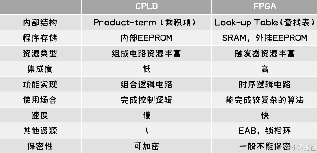
高密度PLD:FPGA与CPLD区别
1、诞生时间:FPGA晚于CPLD
2、适合的领域不同:
FPGA:更适合做运算
CPLD:更适合做控制(内部结构决定)
3、逻辑结构不同:
FPGA:类似于门阵列,拥有较多的触发器和储存器资源
CPLD:CPLD用与或阵列实现的,相当于一大块可编程的与或阵列
4、系统结构:
FPGA:有很多的连接单元,这样虽然让它可以更加灵活的编辑,但是结构却复杂的多。
CPLD:是一个有点限制性的结构。这个结构由一个或者多个可编辑的结果之和的逻辑组列和一些相对少量的锁定的寄存器组成。这样的结果是缺乏编辑灵活性,但是却有可以预计的延迟时间和逻辑单元对连接单元高比率的优点。
5、内部模块不同:
FPGA:其内含有高层次的内置模块(比如加法器和乘法器)和内置的记忆体。很多新的FPGA支持完全的或者部分的系统内重新配置。允许他们的设计随着系统升级或者动态重新配置而改变。一些FPGA可以让设备的一部分重新编辑而其他部分继续正常运行。
6、速度不同
FPGA:速度快
CPLD:速度慢
7、集成度不同
FPGA:集成度高
CPLD:集成度低
HDL:hardware description language 硬件描述语言
ASIC:application specific integrated circuit 专业集成电路
SOC:system on a chip 片上系统
FPGA与ASIC的区别
FPGA:现场可编程门阵列,可编程逻辑IC。这是一种制作时无明确功能,而由用户应用时通过编程来决定功能的数字IC。
ASIC:专用集成电路,一般是面向特定应用领域的IC,如音、视频编解码芯片,网络通信芯片、LCD驱动芯片等。
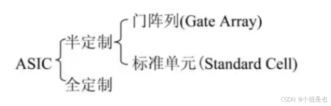
ASIC在市场上总体占有比例比FPGA高,FPGA市场占有比例逐年增长。
2.核心芯片
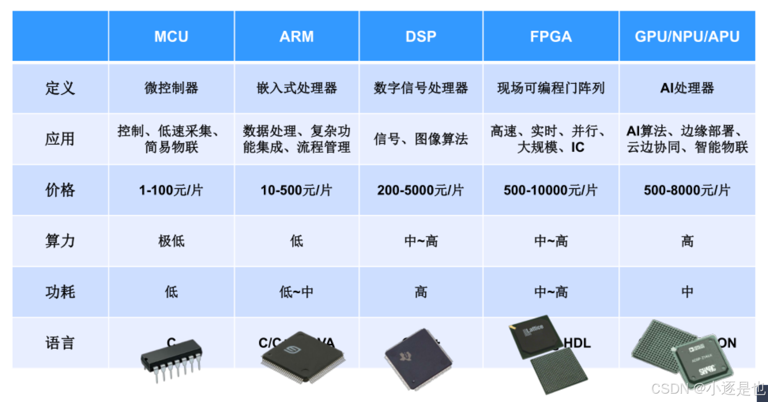
(1)微处理器&微控制器
微控制器:CPU + 片内内存 + 片内外设
处理器通常指微处理器、微控制器和数字信号处理器这三种类型的芯片。
(2)嵌入式系统
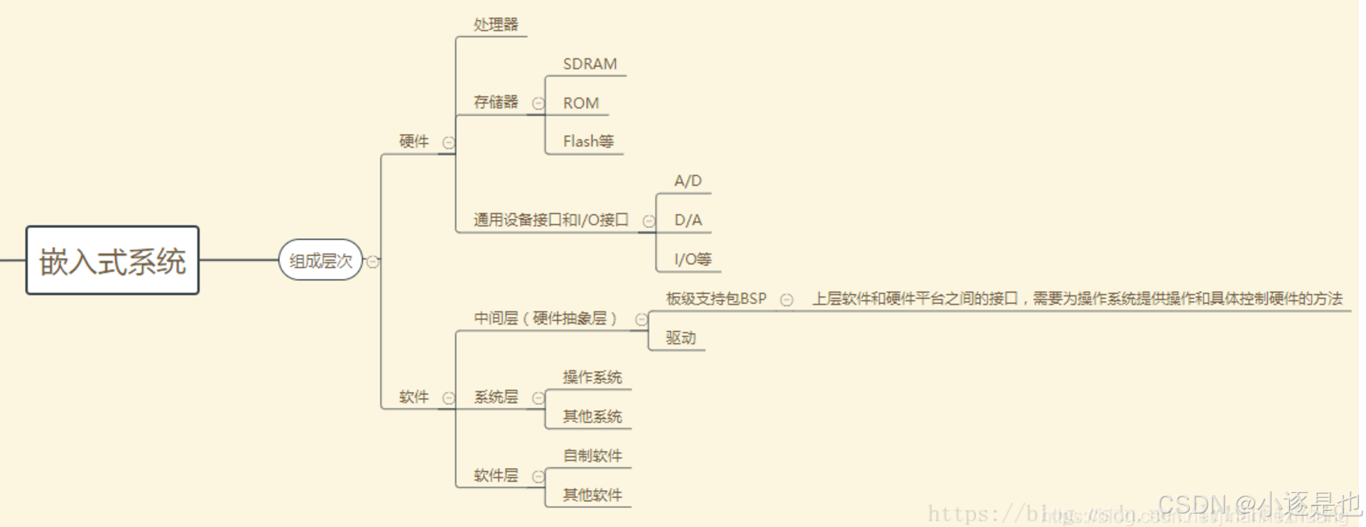
详细了解嵌入式:
(3)数字信号处理器
DSP 即数字信号处理技术, DSP 芯片即指能够实现数字信号处理技术的芯片。 DSP芯片是一种快速强大的微处理器,独特之处在于它能即时处理资料。 DSP 芯片的内部采用程序和数据分开的哈佛结构,具有专门的硬件乘法器,可以用来快速的实现各种数字信号处理算法。 在当今的数字化时代背景下, DSP 己成为通信、计算机、消费类电子产品等领域的基础器件。
详细了解DSP
微控制器和微处理器的区别(含课本原图)_分析微处理器、微控制器、dsp与soc的特点、区别及用途-优快云博客
(4)可编程逻辑器件
可编程逻辑器件 英文全称为:programmable logic device 即 PLD。PLD是做为一种通用集成电路产生的,他的逻辑功能按照用户对器件编程来确定。一般的PLD的集成度很高,足以满足设计一般的数字系统的需要。
CPLD与FPGA的区别可见上文。
3.嵌入式系统分类
4.数字芯片设计思想
搭积木,由一个个简单电路搭建组合
模块化:用少数简单的模块,搭建出复杂各种复杂的功能(IC/IT行业核心思想)
等价性:再复杂的计算都可以等价为很多加减乘除计算,再进而等价为开关电路的逻辑运算,也就是说,实现了后者,前者也就实现了。
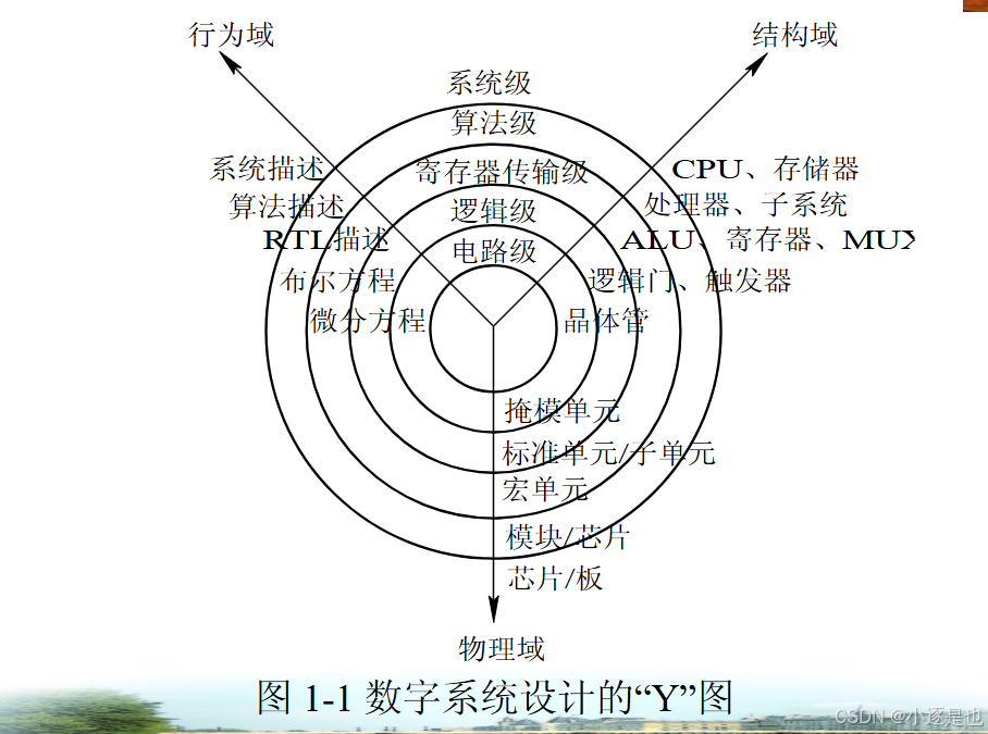
5.EDA的自顶向下设计方法
(1)集成电路与电子系统的设计:定义功能、性能,给出物理实现,满足制约条件,达到最优效用;
(2)一个集成电路或系统的完整性描述,包括行为、结构与物理三个方面;
行为域:电路系统的功能、性能
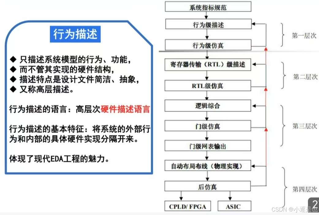
在这一阶段,设计师首先根据需求定义功能模块与规格,然后进行系统的行为级设计。行为描述通常使用硬件描述语言(如VHDL或Verilog)来编写,描述产品的性能和行为。在这个阶段,设计师会编写面向用户的基于逻辑语言的程序,并将其翻译为面向寄存器的程序,最终形成布尔方程组和微分方程。
例如,一个简单的加法器可以使用自然语言描述为“两个输入信号A和B相加,输出结果为S”,然后在行为描述中用代码表示为S = A + B。
结构域:电路系统的逻辑和电路组成
在行为描述的基础上,设计师进一步将系统分解为具体的硬件模块,如CPU、存储器等。然后逐步具体化到寄存器/控制器、逻辑口等部件,最终细化到每一个电容/电阻/晶体管的设计。这一阶段的设计工作从整体出发,逐步具象化到具体的硬件组件。
物理域:电路系统的物理实现
在结构描述完成后,设计师给出芯片的整体设计方案,并在算法层面定义模块之间的连接关系。接着定义宏单元和门级单元图,最终形成物理版图。物理版图是对集成电路的物理情况给出直观、详细的描述。物理设计阶段包括布局和布线,将网表中的逻辑单元和连线布局在芯片上,并连接起来,以满足时序要求。
(3)完成设计是一个从行为到结构到物理的过程。
(4)设计步骤
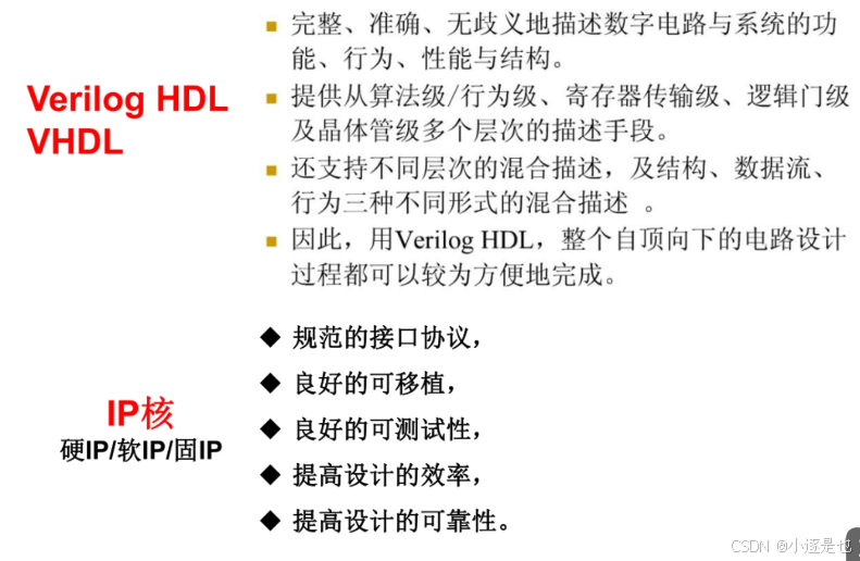
6.Verilog HDL VHDL与IP核
(1) Verilog HDL和VHDL是两种常用的硬件描述语言,广泛应用于数字电路设计中。它们都支持模块化设计、接口定义、状态机和时序设计等关键概念,确保设计的可重用性和功能实现。在FPGA芯片中集成IP核时,通常需要经过编写代码、综合与实现、引入IP核、连接与约束、仿真验证和调试优化等步骤。
IP核(Intellectual Property Core)是一种预先设计好的、经过验证的具有某种确定功能的集成电路模块。IP核有多种形式,包括软核、固核和硬核。软核是功能经过验证的、可综合的HDL模型,固核是在FPGA器件上实现的电路结构编码文件,硬核是在ASIC器件上实现的电路结构掩膜。
在实际应用中,Verilog HDL和VHDL都可以用于生成IP核。例如,在Intel® FPGA IP核的安装、移植与管理指南中提到,可以通过选择VHDL作为输出格式来保留原始输出格式。此外,Altera Corporation提供的Integer Arithmetic IP Cores User Guide中详细介绍了多个IP核的Verilog HDL原型和VHDL组件声明。
在Quartus® II软件中,用户可以通过修改特定TCL脚本文件来生成VHDL IP内核,以解决DisplayPort IP核设计中的问题。Xilinx平台也提供了IP Core生成器(Core Generator),用户可以通过该工具生成各种IP Core,并在Verilog HDL代码中调用这些IP Core。
Verilog HDL和VHDL在数字电路设计中各有优势,用户可以根据具体需求选择合适的语言进行IP核的设计和集成。通过合理的模块化设计和验证过程,可以确保设计的稳定性和可靠性。
二、编程题
11.25:
1.“=”语句记得明确为几进制,输入到输出的连接可以通过“=”实现
与编程语言不同,赋值语句(“连续赋值”)描述事物之间的连接,而不是将值从一个事物复制到另一个事物的操作。
eg:assign one = 1'b1;
eg:assign out= in;
2.两种写法
module new(a)
output a;
endmodule
module new(output a)
endmodule
3.NOTgate
Verilog 有单独的按位 NOT (~) 和逻辑 NOT (!) 运算符,one bit时不做区分
4.ANDgate
Verilog 有单独的按位 AND (&) 和逻辑 AND (&&) 运算符,one bit时不做区分
5.Norgate
Verilog 有单独的按位 OR (|) 和逻辑 OR (||) 运算符,one bit时不做区分
6.XOR
assgin out = a^b;//异或
6.NXOR
assgin out = ~(a^b);//异或
7.Vector0
assign o0 = vec[0];
assign o1 = vec[1];
assign o2 = vec[2];
向量展开// This is ok too: assign {o2, o1, o0} = vec;
8.Vector1
wire作输入输出,组合逻辑
reg可作中间存储变量,通常用于时序逻辑中
-
组合逻辑(Combinational Logic):
-
组合逻辑电路的输出仅取决于当前输入信号的状态,与电路的先前状态无关。这意味着,一旦输入信号发生变化,输出会立即响应并更新。
-
组合逻辑电路通常由逻辑门(如与门、或门、非门等)构成,没有存储单元,因此不存在反馈回路。
-
常见的组合逻辑电路包括加法器、编码器、译码器、数据选择器和数值比较器等。
-
组合逻辑电路容易出现竞争冒险现象,即在输入信号变化时可能会产生瞬时的不稳定性或毛刺。
-
-
时序逻辑(Sequential Logic):
-
时序逻辑电路的输出不仅取决于当前输入信号,还与电路的内部状态有关。这种状态通常由存储元件(如触发器)来保存。
-
时序逻辑电路的行为受到时钟信号的控制,通常在时钟的上升沿或下降沿触发输出的变化。
-
常见的时序逻辑电路包括寄存器、移位寄存器、计数器和状态机等。
-
由于时序逻辑电路具有记忆功能,因此它们能够处理更复杂的任务,如序列控制和状态管理。
-
eg:
wire [7:0] w;         // 8-bit wire
reg  [4:1] x;         // 4-bit reg
output reg [0:0] y;   // 1-bit reg that is also an output port (this is still a vector)
input wire [3:-2] z;  // 6-bit wire input (negative ranges are allowed)
output [3:0] a;       // 4-bit output wire. Type is 'wire' unless specified otherwise.
wire [0:7] b;         // 8-bit wire where b[0] is the most-significant bit.
-
隐式网络的定义:
- 在Verilog中,可以通过
assign语句隐式地创建网类型信号(wire)。 - 当将未声明的信号连接到模块端口时,也会隐式创建一个单比特的网类型信号。
- 这些隐式创建的信号始终是单比特的wire,这可能会导致问题,特别是当你期望使用一个向量(多比特信号)时,隐式网会导致难以发现的错误。
`default_nettype none // 禁用隐式网络的创建

wire [2:0] a, c;   // 两个向量
assign a = 3'b101;  // a = 101
assign b = a;       // b = 1 (隐式创建的wire)
assign c = b;       // c = 001 <-- bug
my_module i1 (d,e); // d和e如果未声明,则隐式为1位宽
                    // 如果该端口是一个向量,这里就会出现bug
- 在Verilog中,可以通过
9.Vectorgates
module top_module(
    input [2:0] a,
    input [2:0] b,
    output [2:0] out_or_bitwise,
    output out_or_logical,
    output [5:0] out_not
);
    assign out_or_bitwise = a|b;//按位或
    assign out_or_logical = a||b;//逻辑或
    assign out_not = {~b,~a};//按位连接符
   //This is ok too:
   //assign out_not[2:0] = ~a;	// Part-select on left side is o.
   //assign out_not[5:3] = ~b;	//Assigning to [5:3] does not conflict with [2:0]


endmodule-
逻辑或:假设
a = true,b = false,那么a || b的结果为true。因为逻辑或只需要一个操作数为真即可返回真,且具有短路特性,所以不会计算b的值。 -
按位或:假设
a = 5(二进制为0101),b = 3(二进制为0011),那么a | b的结果为7(二进制为0111)。这是因为按位或会逐位进行或运算,只要有一个位为1,结果的对应位就为1。
10.
module top_module(
    input [3:0] in,
    output out_and,
    output out_or,
    output out_xor
);
    assign out_and = in[0]&in[1]&in[2]&in[3];//AND
    assign out_or = in[0]|in[1]|in[2]|in[3];//OR
    assign out_xor = in[0]^in[1]^in[2]^in[3];//XOR 异或 Exclusive OR

endmodule
11.
Concatenation 需要知道每个组件的宽度(或者你怎么知道结果的长度?因此,{1, 2, 3} 是非法的,并导致错误消息:串联中不允许使用未调整大小的常量。
input [15:0] in;
output [23:0] out;
assign {out[7:0], out[15:8]} = in;         // Swap two bytes. Right side and left side are
                                              both 16-bit vectors.
assign out[15:0] = {in[7:0], in[15:8]};    // This is the same thing.
assign out = {in[7:0], in[15:8]};       // 由于位数不匹配 需要进行位扩展This is different.
                                            The 16-bit vector on the
                                          right is extended to
                                        // match the 24-bit vector on the left, so
                                         out[23:16] are zero.
                                        // In the first two examples, out[23:16] are not assigned.
12.
module top_module (
    input [4:0] a, b, c, d, e, f,
    output [7:0] w, x, y, z );//

    assign {w[7:0]} = {a,b[4:2]};
    assign {x[7:0]} = {b[1:0],c,d[4]};
    assign {y[7:0]} = {d[3:0],e[4:1]};
    assign z = {e[0],f,2'b11};

endmodule

//assign {w,x,y,z} = {a,b,c,d,e,f,2'b11};
13.
assign out[7:0] = in[0:7]; does not work because Verilog does not allow vector bit ordering to be flipped.
The concatenation operator may save a bit of coding, allowing for 1 assign statement instead of 8.

//不允许翻转操作out[7:0] = in[0:7];
正确解法:
module top_module(
    input [7:0] in,
    output [7:0] out
);
    assign out= {in[0],in[1],in[2],in[3],in[4],in[5],in[6],in[7]};
endmodule
14.
module top_module (
    input a, b, c, d, e,
    output [24:0] out );//
    assign out = ~{{5{a}},{5{b}},{5{c}},{5{d}},{5{e}}}^{5{a,b,c,d,e}};
    // The output is XNOR of two vectors created by
    // concatenating and replicating the five inputs.
    // assign out = ~{ ... } ^ { ... };

endmodule
异或:相同为0,不同为1;所以本题要进行取反按位取反
15.实例化一个模块
module top_module ( input a, input b, output out );
    mod_a instance1(.out(out),.in1(a),.in2(b));//按名称
endmodule


参考答案:
module top_module (
	input a,
	input b,
	output out
);

	// Create an instance of "mod_a" named "inst1", and connect ports by name:
	mod_a inst1 (
		.in1(a), 	// Port"in1"connects to wire "a"
		.in2(b),	// Port "in2" connects to wire "b"
		.out(out)	// Port "out" connects to wire "out"
				// (Note: mod_a's port "out" is not related to top_module's wire "out".
				// It is simply coincidence that they have the same name)
	);

/*
	// Create an instance of "mod_a" named "inst2", and connect ports by position:
	mod_a inst2 ( a, b, out );	// The three wires are connected to ports in1, in2, and out, respectively.
*/

endmodule
16.
module top_module ( input clk, input d, output q );
wire q0,q1;
my_dff ins1(clk,d,q0);
my_dff ins2(clk,q0,q1);
my_dff ins3(clk,q1,q);
endmodule
17.
module top_module (
    input clk,
    input [7:0] d,
    input [1:0] sel,
    output [7:0] q
);
    wire [7:0]a0,a1,a2;
    my_dff8 inst1(clk,d,a0);
    my_dff8 inst2(clk,a0,a1);
    my_dff8 inst3(clk,a1,a2);
    always@(*)
        begin
            case(sel)
                2'b00:q=d;
                2'b01:q=a0;
                2'b10:q=a1;
                2'b11:q=a2;
            endcase
        end

endmodule
18.
module top_module(
    input [31:0] a,
    input [31:0] b,
    output [31:0] sum
);
    wire [15:0] sum1,sum2;
    wire cout1,cout2;
    reg cin;
    assign cin=0;
    add16 inst1(.sum(sum1),.cout(cout1),.cin(cin),.a(a[15:0]),.b(b[15:0]));
    add16 inst2(.sum(sum2),.cout(cout2),.cin(cout1),.a(a[31:16]),.b(b[31:16]));
    assign sum={sum2,sum1};

endmodule
19.
module top_module (
    input [31:0] a,
    input [31:0] b,
    output [31:0] sum
);
    wire cout1,cout2;
    wire [15:0] sum1,sum2;
    add16 low(.a(a[15:0]),.b(b[15:0]),.cin(16'b0),.sum(sum1),.cout(cout1));
    add16 hi(.a(a[31:16]),.b(b[31:16]),.cin(cout1),.sum(sum2),.cout(cout2));
    assign sum={sum2,sum1};
//

endmodule

module add1 ( input a, input b, input cin,   output sum, output cout );
    always@(*)
        begin
            case({a,b,cin})
                 3'b000:{sum,cout}=2'b00;
                 3'b001:{sum,cout}=2'b10;
                 3'b010:{sum,cout}=2'b10;
                 3'b011:{sum,cout}=2'b01;
                 3'b100:{sum,cout}=2'b10;
                 3'b101:{sum,cout}=2'b01;
                 3'b110:{sum,cout}=2'b01;
                 3'b111:{sum,cout}=2'b11;
            endcase
        end


endmodule
20.
module top_module(
    input [31:0] a,
    input [31:0] b,
    output [31:0] sum
);
    wire [15:0]sum1,sum2,sum3;
    wire cout1,cout2,cout3;
    add16 ad1(.a(a[15:0]),.b(b[15:0]),.cin(16'b00),.sum(sum1[15:0]),.cout(cout1));
    add16 ad2(.a(a[31:16]),.b(b[31:16]),.cin(16'b00),.sum(sum2[15:0]),.cout(cout2));
    add16 ad3(.a(a[31:16]),.b(b[31:16]),.cin(16'b01),.sum(sum3[15:0]),.cout(cout3));
                                  always@(*)
                                      begin
                                          case(cout1)
                                              0:sum={sum2,sum1};
                                              1:sum={sum3,sum1};
                                          endcase
                                      end

endmodule
21.
module top_module(
    input [31:0] a,
    input [31:0] b,
    input sub,
    output [31:0] sum
);
    wire [31:0]b1;
    wire [15:0]sum1,sum2;
    wire cout0,cout1;
    add16 inst1(.a(a[15:0]),.b(b1[15:0]),.cin(sub),.cout(cout0),.sum(sum1));
    add16 inst2(.a(a[31:16]),.b(b1[31:16]),.cin(cout0),.cout(cout1),.sum(sum2));
    assign b1=b^{32{sub}};
    assign sum={sum2,sum1};
endmodule
22.assign与always
// synthesis verilog_input_version verilog_2001
module top_module(
    input a,
    input b,
    output wire out_assign,
    output reg out_alwaysblock
);
    assign out_assign = a&b;
    always@(*)
        begin
            out_alwaysblock=a&b;
        end

endmodule
23.阻塞与非阻塞
1).非阻塞(Non_Blocking)赋值方式( 如 b <= a; )
块结束后才完成赋值操作。
b的值并不是立刻就改变的。
这是一种比较常用的赋值方法。(特别在编写可综合模块时)
(2).阻塞(Blocking)赋值方式( 如 b = a; )
赋值语句执行完后,块才结束。
b的值在赋值语句执行完后立刻就改变的。
可能会产生意想不到的结果。
24.
// synthesis verilog_input_version verilog_2001
module top_module(
    input a,
    input b,
    input sel_b1,
    input sel_b2,
    output wire out_assign,
    output reg out_always   );
    assign out_assign = (sel_b1&sel_b2)?b:a;
    always@(*)
        begin
        case({sel_b1,sel_b2})

                2'b00:out_always=a;
                2'b01:out_always=a;
                2'b10:out_always=a;
                2'b11:out_always=b;
        endcase
        end

endmodule
25.else_if成对出现
// synthesis verilog_input_version verilog_2001
module top_module (
    input      cpu_overheated,
    output reg shut_off_computer,
    input      arrived,
    input      gas_tank_empty,
    output reg keep_driving  ); //

    always @(*) begin
        if (cpu_overheated)
           shut_off_computer = 1;
        else
            shut_off_computer = 0;
    end

    always @(*) begin
        if (~arrived)
           keep_driving = ~gas_tank_empty;
        else
           keep_driving = 0;
    end

endmodule
always语句后紧跟begin
26.比大小
module top_module (
    input [7:0] a, b, c, d,
    output [7:0] min);//
    wire [7:0] min1,min2;
    assign min1=(a>b)?b:a;
    assign min2=(c>d)?d:c;
    assign min=(min1>min2)?min2:min1;
    // assign intermediate_result1 = compare? true: false;

endmodule
27.
module top_module(
    input [399:0] a, b,
    input cin,
    output cout,
    output [399:0] sum );
    reg [99:0]cout1;
    bcd_fadd inst[99:0](.a(a[399:0]),.b(b[399:0]),.cin({cout1[98:0],cin}),.cout(cout1[99:0]),.sum(sum[399:0]));
    assign cout = cout1[99];


endmodule
实例化电路
bcd_fadd inst[99:0](.a(a[399:0]),.b(b[399:0]),.cin({cout1[98:0],cin}),.cout(cout1[99:0]),.sum(sum[399:0]));
即产生100个bcd加法器
26.
module top_module(
    input x3,
    input x2,
    input x1,  // three inputs
    output f   // one output
);
    always@(*)
        begin
            case({x3,x2,x1})
                3'b000: f=0;
                3'b001: f=0;
                3'b010: f=1;
                3'b011: f=1;
                3'b100: f=0;
                3'b101: f=1;
                3'b110: f=0;
                3'b111: f=1;
               endcase
         end

endmodule


//解法2
module top_module (
	input x3,
	input x2,
	input x1,
	output f
);
	// This truth table has four minterms.
	assign f = ( ~x3 & x2 & ~x1 ) |
				( ~x3 & x2 & x1 ) |
				( x3 & ~x2 & x1 ) |
				( x3 & x2 & x1 ) ;

	// It can be simplified, by boolean algebra or Karnaugh maps.
	// assign f = (~x3 & x2) | (x3 & x1);

	// You may then notice that this is actually a 2-to-1 mux, selected by x3:
	// assign f = x3 ? x1 : x2;

endmodule
27.
module top_module(
	input [1:0] A,
	input [1:0] B,
	output z);

	assign z = (A[1:0]==B[1:0]);	// Comparisons produce a 1 or 0 result.

	// Another option is to use a 16-entry truth table ( {A,B} is 4 bits, with 16 combinations ).
	// There are 4 rows with a 1 result.  0000, 0101, 1010, and 1111.

endmodule
28.
module top_module (input x, input y, output z);

    wire z1,z2,z3,z4;

    A IA1(.x(x),.y(y),.z(z1));
    B IB1(.x(x),.y(y),.z(z2));
    A IA2(.x(x),.y(y),.z(z3));
    B IB2(.x(x),.y(y),.z(z4));
    assign z=(z1|z2)^(z3&z4);
endmodule
module A (input x, input y, output z);
    assign z = (x^y) & x;
endmodule

module B ( input x, input y, output z );
    assign z = ~x^y;
endmodule
29.
module top_module (
    input ring,
    input vibrate_mode,
    output ringer,       // Make sound
    output motor         // Vibrate
);
    assign ringer = (ring & ~vibrate_mode)? 1 : 0;//来电且没开振动 响铃
    assign motor = (ring & vibrate_mode)? 1 : 0;


endmodule
30.
module top_module(
	input too_cold,
	input too_hot,
	input mode,
	input fan_on,
	output heater,
	output aircon,
	output fan
);
	// Reminder: The order in which you write assign statements doesn't matter.
	// assign statements describe circuits, so you get the same circuit in the end
	// regardless of which portion you describe first.

	// Fan should be on when either heater or aircon is on, and also when requested to do so (fan_on = 1).
	assign fan = heater | aircon | fan_on;

	// Heater is on when it's too cold and mode is "heating".
	assign heater = (mode & too_cold);

	// Aircon is on when it's too hot and mode is not "heating".
	assign aircon = (~mode & too_hot);

	// * Unlike real thermostats, there is no "off" mode here.

endmodule
31.有多少个1
module top_module(
    input [2:0] in,
    output [1:0] out );
    integer i ;
    always@(*)

        begin
            out=0;
            for(i=0;i<3;i++)
              begin
                if(in[i]==1)
                   out=out+1;
              end
        end

endmodule

//解2
module top_module (
	input [2:0] in,
	output [1:0] out
);

	// This is a function of 3 inputs. One method is to use a 8-entry truth table:
	// in[2:0] out[1:0]
	// 000      00
	// 001      01
	// 010      01
	// 011      10
	// 100      01
	// 101      10
	// 110      10
	// 111      11
	assign out[0] = (~in[2] & ~in[1] & in[0]) | (~in[2] & in[1] & ~in[0]) | (in[2] & ~in[1] & ~in[0]) | (in[2] & in[1] & in[0]);
	assign out[1] = (in[1] & in[0]) | (in[2] & in[0]) | (in[2] & in[1]);

	// Using the addition operator works too:
	// assign out = in[0]+in[1]+in[2];

	// Yet another method uses behavioural code inside a procedure (combinational always block)
	// to directly implement the truth table:
	/*
	always @(*) begin
		case (in)
			3'd0: out = 2'd0;
			3'd1: out = 2'd1;
			3'd2: out = 2'd1;
			3'd3: out = 2'd2;
			3'd4: out = 2'd1;
			3'd5: out = 2'd2;
			3'd6: out = 2'd2;
			3'd7: out = 2'd3;
		endcase
	end//空间换时间
	*/

endmodule
32.
module top_module(
    input [3:0] in,
    output [2:0] out_both,
    output [3:1] out_any,
    output [3:0] out_different );

    integer i;
    always@(*)
        begin
            out_both=0;
            out_any=0;
            out_different=0;
            out_different[3]=in[0]^in[3];

            for(i=0;i<3;i++)
                begin
                    out_both[i]=in[i]&in[i+1];
                    out_any[i+1]=in[i+1]|in[i];
                    out_different[i]=in[i]^in[i+1];
                end
        end

endmodule
//解2
module top_module (
	input [3:0] in,
	output [2:0] out_both,
	output [3:1] out_any,
	output [3:0] out_different
);

	// Use bitwise operators and part-select to do the entire calculation in one line of code
	// in[3:1] is this vector:   					 in[3]  in[2]  in[1]
	// in[2:0] is this vector:   					 in[2]  in[1]  in[0]
	// Bitwise-OR produces a 3 bit vector.			   |      |      |
	// Assign this 3-bit result to out_any[3:1]:	o_a[3] o_a[2] o_a[1]

	// Thus, each output bit is the OR of the input bit and its neighbour to the right:
	// e.g., out_any[1] = in[1] | in[0];
	// Notice how this works even for long vectors.
	assign out_any = in[3:1] | in[2:0];

	assign out_both = in[2:0] & in[3:1];

	// XOR 'in' with a vector that is 'in' rotated to the right by 1 position: {in[0], in[3:1]}
	// The rotation is accomplished by using part selects[] and the concatenation operator{}.
	assign out_different = in ^ {in[0], in[3:1]};

endmodule
错位运算
33.
module top_module(
    input [99:0] in,
    output [98:0] out_both,
    output [99:1] out_any,
    output [99:0] out_different );

    assign out_both=in[98:0]&in[99:1];
    assign out_any=in[98:0]|in[99:1];
    assign out_different=in[99:0]^{in[0],in[99:1]};
endmodule
34.
module top_module(
    input a, b, sel,
    output out );

    assign out = sel?b:a;
endmodule
35.
module top_module(
    input [15:0] a, b, c, d, e, f, g, h, i,
    input [3:0] sel,
    output [15:0] out );

    always@(*)
        begin
            case(sel)
                    0:out=a;
                    1:out=b;
                    2:out=c;
                    3:out=d;
                    4:out=e;
                    5:out=f;
                    6:out=g;
                    7:out=h;
                    8:out=i;
                    default:out=16'b11111111111111111111;//16'hffff
                    endcase

        end
endmodule
36.
module top_module(
    input a, b, cin,
    output cout, sum );

    assign sum =a^b^cin;
    assign cout =a&b|(cin&(a^b));
endmodule
37.
module top_module(
    input [2:0] a, b,
    input cin,
    output [2:0] cout,
    output [2:0] sum );

    wire cout1,cout2,cout3;
    adder inst1(.a(a[0]),.b(b[0]),.cin(cin),.cout(cout[0]),.sum(sum[0]));
    adder inst2(.a(a[1]),.b(b[1]),.cin(cout[0]),.cout(cout[1]),.sum(sum[1]));
    adder inst3(.a(a[2]),.b(b[2]),.cin(cout[1]),.cout(cout[2]),.sum(sum[2]));
endmodule

module adder(
    input a, b,
    input cin,
    output  cout,
    output  sum );
    assign sum=a^b^cin;
    assign cout = a&b|cin&(a^b);

endmodule
38.全加器与生成实例
module top_module (
    input [3:0] x,
    input [3:0] y,
    output [4:0] sum);
    wire cout0,cout1,cout2,cout3;
    FA inst0(.x(x[0]),.y(y[0]),.cin(1'b0),.sum(sum[0]),.cout(cout0));
    FA inst1(.x(x[1]),.y(y[1]),.cin(cout0),.sum(sum[1]),.cout(cout1));
    FA inst2(.x(x[2]),.y(y[2]),.cin(cout1),.sum(sum[2]),.cout(cout2));
    FA inst3(.x(x[3]),.y(y[3]),.cin(cout2),.sum(sum[3]),.cout(cout3));
    assign sum[4] = cout3;

endmodule
module FA(input x,input y,input cin,output sum,output cout);
    assign sum = x^y^cin;
    assign cout = x&y|(cin&(x^y));
endmodule
39.
module top_module (
    input [7:0] a,
    input [7:0] b,
    output [7:0] s,
    output overflow
);
    wire c;
    assign {c,s} = a+b; //构建加法器
    assign overflow=a[7] & b[7] & ~s[7] | ~a[7] & ~b[7] & s[7];
//溢出
//eg a = 3'b011;
//b = 3'b001;
//两者均为正数时,sum = 3'100;
//结果为复数
//1.情况一 ~a[3]&~b[3]&sum[3] =1;出现溢出
//2.情况二 a[3]&b[3]&~sum[3] =1;出现溢出
//以此类推 assign overflow=a[7] & b[7] & ~s[7] | ~a[7] & ~b[7] & s[7];
endmodule
40.创建一个 100 位二进制加法器。加法器将两个 100 位数字和一个 carry-in 相加,以产生 100 位求和并执行。
module top_module(
    input [99:0] a, b,
    input cin,
    output cout,
    output [99:0] sum );
    assign {cout,sum} = a+b+cin;
endmodule
//直接构建加法器,assign语句
41.
module top_module (
    input [15:0] a, b,
    input cin,
    output cout,
    output [15:0] sum );

    wire cout1[3:0];
    bcd_fadd inst1(.a(a[3:0]),.b(b[3:0]),.cin(cin),.cout(cout1[0]),.sum(sum[3:0]));
    bcd_fadd inst2(.a(a[7:4]),.b(b[7:4]),.cin(cout1[0]),.cout(cout1[1]),.sum(sum[7:4]));
    bcd_fadd inst3(.a(a[11:8]),.b(b[11:8]),.cin(cout1[1]),.cout(cout1[2]),.sum(sum[11:8]));
    bcd_fadd inst4(.a(a[15:12]),.b(b[15:12]),.cin(cout1[2]),.cout(cout1[3]),.sum(sum[15:12]));
    assign cout = cout1[3];
endmodule
42.
=赋值操作符:- 立即赋值:
=是阻塞赋值操作符,它会立即执行赋值操作,并且新值可以立即在后续的语句中使用。这意味着在赋值语句执行后,新值会立即生效。 - 适用场景:通常用于组合逻辑(combinational logic)中。组合逻辑是指输出仅依赖于当前输入的逻辑电路。例如,在
always @(*)块中使用=进行赋值.
- 立即赋值:
<=赋值操作符:- 延迟赋值:
<=是非阻塞赋值操作符,它不会立即执行赋值操作,而是等到当前时间步的所有非阻塞赋值操作都完成后才进行赋值。这意味着新值不会立即生效,而是在当前时间步的所有非阻塞赋值操作完成后才更新。 - 适用场景:通常用于时序逻辑(sequential logic)中。时序逻辑是指输出不仅依赖于当前输入,还依赖于过去的输入或状态。例如,在
always @(posedge clk)块中使用<=进行赋值。
- 延迟赋值:
43.
D(decimal)表示这个数是十进制
B(binary)表示这个数是二进制
O(octor)表示这个数是八进制
H(hex)表示这个数是十六进制
44.
module top_module (
    input clk,
    input resetn,
    input [1:0] byteena,
    input [15:0] d,
    output [15:0] q
);
    always@(posedge clk)
        begin
            if(resetn==0)
                q<=0;
            else if (byteena[1] | byteena[0])
                begin
            if (byteena[1])
                q[15:8] <= d[15:8];
            if (byteena[0])
                q[7:0] <= d[7:0];
        end


        end

endmodule
45.
module top_module (
    input clk,
    input w, R, E, L,
    output Q
);

    wire si,temp;
    assign si=E?w:Q;
    assign temp=L?R:si;
    always@(posedge clk)
        begin
            Q<=temp;
        end
endmodule
//assign temp = L ? R :(E ? w : Q);二选一语句的应用
46.
module top_module (
    input clk,
    input x,
    output z
);
    reg q1,q2,q3;
    always@(posedge clk)
        begin
            q1<=x^q1;
            q2<=x&(~q2);
            q3<=x|(~q3);

        end

    assign z=~(q1|q2|q3);
endmodule
47.
//解法1
module top_module (
    input clk,
    input j,
    input k,
    output Q);

    always@(posedge clk)begin
        case({j,k})
            2'b00:	Q <= Q;
            2'b01:	Q <= 1'b0;
            2'b10:	Q <= 1'b1;
            2'b11:	Q <= ~Q;
            default:;
        endcase
    end

endmodule
//解法2
module top_module (
    input clk,
    input j,
    input k,
    output Q);

    always@(posedge clk)
        begin
            if(j^k)
                Q<=j;
            else if(j==0&k==0)
                Q<=Q;
            else
                Q<=~Q;
        end
endmodule
48.
FPGA实现边沿检测电路(上升沿、下降沿)_上升沿检测电路-优快云博客
module top_module (
input clk,
input [7:0] in,
output [7:0] pedge
);
reg [7:0]in1;
always@(posedge clk)
begin
in1<=in;//存一拍
pedge<=~in1∈
end
endmodule
看图发现错位一拍出现信号
49.
module top_module (
    input clk,
    input reset,
    input [31:0] in,
    output [31:0] out
);
    reg [31:0] in1;
    always@(posedge clk)
        begin
            in1<=in;
            if(reset)
              out<=0;
            else
                out<=~in&(in1)|out;//下降沿检测or保持原样
        end

endmodule
50.
module top_module(
    input clk,
    input areset,  // async active-high reset to zero
    input load,
    input ena,
    input [3:0] data,
    output reg [3:0] q);
    always@(posedge clk or posedge areset)
        begin
            if(areset)
                q<=0;
            else if(load)
                q<=data;
            else if(ena)
                q<={1'b0,q[3:1]};
            else
                q<=q;
        end

endmodule
60.
module top_module(
    input clk,
    input load,
    input ena,
    input [1:0] amount,
    input [63:0] data,
    output reg [63:0] q);

    always@(posedge clk)
        begin
            if(load)
                q<=data;
            else if(ena)
                begin
                    case(amount)
                        2'b00:q<={q[62:0],1'b0};
                        2'b01:q<={q[55:0],8'b0};
                        2'b10:q<={q[63],q[63:1]};
                        2'b11:q<={{8{q[63]}},q[63:8]};
                        default:q<=q;
                    endcase
                end
        end
endmodule
61. 结:左移不需要保留符号位,右移高位由符号位补充
module top_module(
    input clk,
    input load,
    input [1:0] ena,
    input [99:0] data,
    output reg [99:0] q);
    always@(posedge clk)
        begin
            if(load)
                q<=data;
            else
                begin
                    case(ena)
                        2'b01:q<={q[0],q[99:1]};
                        2'b10:q<={q[98:0],q[99]};
                        default:q<=q;
                    endcase
                end
        end

endmodule
62.
module top_module(
    input clk,
    input reset,    // Active-high synchronous reset to 5'h1
    output [4:0] q
);
    always@(posedge clk)
        begin
            if(reset)
                q<=5'h1;
            else
                begin
                    q[4]<=1'b0^q[0];
                    q[3]<=q[4];
                    q[2]<=q[3]^q[0];
                    q[1]<=q[2];
                    q[0]<=q[1];
                end
        end

endmodule
63.
module top_module (
	input [2:0] SW,      // R
	input [1:0] KEY,     // L and clk
	output [2:0] LEDR);  // Q

    always@(posedge KEY[0])
        begin
            LEDR = KEY[1]?SW:{LEDR[2]^LEDR[1],LEDR[0],LEDR[2]};
        end

endmodule
64.
module top_module (
    input clk,
    input resetn,   // synchronous reset
    input in,
    output out);
    reg q0,q1,q2;
    dd inst1(in,clk,resetn,q0);
    dd inst2(q0,clk,resetn,q1);
    dd inst3(q1,clk,resetn,q2);
    dd inst4(q2,clk,resetn,out);

endmodule
module dd(input in,input clk,input reset,output q);
    always@(posedge clk)
        begin
            if(~reset)
                q<=0;
            else
                q<=in;
        end
endmodule

//解2
module top_module (
	input clk,
	input resetn,
	input in,
	output out
);

	reg [3:0] sr;

	// Create a shift register named sr. It shifts in "in".
	always @(posedge clk) begin
		if (~resetn)		// Synchronous active-low reset
			sr <= 0;
		else
			sr <= {sr[2:0], in};
	end

	assign out = sr[3];		// Output the final bit (sr[3])

endmodule
65.
module top_module(
    input in,
    input [1:0] state,
    output [1:0] next_state,
    output out); //
    parameter A=0, B=1, C=2, D=3;

    always@(*)
        begin
            case(state)
                A:begin next_state=in?B:A;
                    out=0;
                end
                B:begin next_state=in?B:C;
                    out=0;
                end
                C:begin
                    next_state=in?D:A;
                    out=0;
                end
                D:begin
                    next_state=in?B:C;
                    out=1;
                end
            endcase
        end

endmodule
66.
module top_module(
    input clk,
    input areset,    // Freshly brainwashed Lemmings walk left.
    input bump_left,
    input bump_right,
    output walk_left,
    output walk_right); //

    parameter LEFT=0, RIGHT=1;
    reg state, next_state;

    always @(*) begin
        case(state)
           LEFT: next_state=bump_left? RIGHT:LEFT;
           RIGHT:next_state=bump_right? LEFT:RIGHT;
        endcase
    end

    always @(posedge clk, posedge areset) begin
        if(areset)
            state<=LEFT;
        else
            state<=next_state;
    end

     assign walk_left = (state == LEFT);
     assign walk_right = (state == RIGHT);


endmodule
67.
module top_module(
    input clk,
    input areset,    // Freshly brainwashed Lemmings walk left.
    input bump_left,
    input bump_right,
    input ground,
    output walk_left,
    output walk_right,
    output aaah );

    parameter LEFT=0;
    parameter RIGHT=1;
    parameter FALL_L=2;
    parameter FALL_R=3;
    reg [1:0]state,next_state;
    always@(*)
        begin
            case(state)
                LEFT: next_state= (~ground)?(FALL_L):(bump_left?RIGHT:LEFT);
                RIGHT:next_state= (~ground)?(FALL_R):(bump_right?LEFT:RIGHT);
                FALL_L:next_state= ground?(LEFT):(FALL_L);
                FALL_R:next_state= ground?(RIGHT):(FALL_R);
            endcase
        end
    always@(posedge clk or posedge areset)
        begin
           if(areset)
               state<=LEFT;
            else
                state<=next_state;
        end
    assign walk_left = (state==LEFT);
    assign walk_right = (state==RIGHT);
    assign aaah = (state==FALL_L|state==FALL_R);
endmodule
68.
module top_module(
    input clk,
    input areset,    // Freshly brainwashed Lemmings walk left.
    input bump_left,
    input bump_right,
    input ground,
    input dig,
    output walk_left,
    output walk_right,
    output aaah,
    output digging );

    parameter LEFT=0;
    parameter RIGHT=1;
    parameter FALL_L=2;
    parameter FALL_R=3;
    parameter DIG_L=4;
    parameter DIG_R=5;
    reg [3:0]state,next_state;
    always@(*)
        begin
            case(state)
                LEFT: next_state= (~ground)?(FALL_L):(dig?DIG_L:(bump_left?RIGHT:LEFT));
                RIGHT:next_state= (~ground)?(FALL_R):(dig?DIG_R:(bump_right?LEFT:RIGHT));
                FALL_L:next_state= ground?(LEFT):(FALL_L);
                FALL_R:next_state= ground?(RIGHT):(FALL_R);
                DIG_L: next_state=(ground)?DIG_L:FALL_L;
                DIG_R: next_state=(ground)?DIG_R:FALL_R;
            endcase
        end
    always@(posedge clk or posedge areset)
        begin
           if(areset)
               state<=LEFT;
            else
                state<=next_state;
        end
    assign walk_left = (state==LEFT);
    assign walk_right = (state==RIGHT);
    assign aaah = (state==FALL_L|state==FALL_R);
    assign digging = (state==DIG_L|state==DIG_R);
endmodule
69.
module top_module(
    input in,
    input [9:0] state,
    output [9:0] next_state,
    output out1,
    output out2);

    assign next_state[0] = ~in & (state[0]|state[1]|state[2]|state[3]|state[4]|state[7]|state[8]|state[9]);
    assign next_state[1] = in & (state[0]|state[8]|state[9]);
    assign next_state[2] = in & state[1];
    assign next_state[3] = in & state[2];
    assign next_state[4] = in & state[3];
    assign next_state[5] = in & state[4];
    assign next_state[6] = in & state[5];
    assign next_state[7] = in & (state[6]|state[7]);
    assign next_state[8] = ~in & state[5];
    assign next_state[9] = ~in & state[6];

    assign out1 = state[8]|state[9];
    assign out2 = state[7]|state[9];
endmodule
70.
module top_module(
    input clk,
    input [7:0] in,
    input reset,    // Synchronous reset
    output done); //

    // State transition logic (combinational)
   parameter [1:0] First_state=2'b00, Second_state=2'b01, Third_state=2'b10, Wait_state=2'b11;
   reg [1:0] state, next_state;

    always @(*) begin
        case(state)     // State transition logic
            First_state:
                next_state <= Second_state;
           Second_state:
                next_state <= Third_state;
		   Third_state:begin
               if(in[3] == 1'b1)
                next_state <= First_state;
               else
                next_state <= Wait_state;
               end
           Wait_state:begin
               if(in[3] == 1'b1)
                next_state <= First_state;
               else
                next_state <= Wait_state;
               end
        endcase
    end

    // State flip-flops (sequential)
    always @(posedge clk) begin
        if(reset)
            state <= Wait_state;
        else
            state <= next_state;
    end

    // Output logic
    assign done = (state == Third_state);

endmodule


 3817
3817

 被折叠的 条评论
为什么被折叠?
被折叠的 条评论
为什么被折叠?
 到【灌水乐园】发言


