


 本文详细介绍了FPGA设计中的综合步骤,包括库的指定、设计文件的读取和约束设置,如时序和面积约束、环境属性约束、设计规则等。此外,还探讨了时序分析的关键,以及从架构级到门级的优化策略。最后,提到了编译策略和解决时序问题的方法,为FPGA开发提供了深入的指导。
文章目录
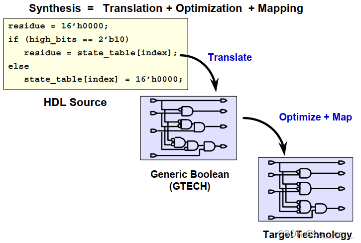
⭐Synthesis = Translation + Optimization + Mapping
⭐综合步骤
1.指定相关的库
set target_library "my_tech.db"
set link_library "* my_tech.db"
set symbol_library "tc6a.sdb"
2.读取设计文件
analyze -f verilog ALU.v
analyze -f verilog TOP.v
elaborate TOP
check_design
3.相关约束
3.1Timing and Area相关约束
- area:
set_max_area 0 - timing
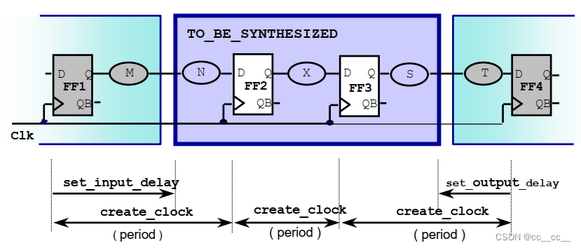
create_clock -period 10 [get_ports clk]
set_dont_touch_network [get_clocks clk]  # not to buffer up the clock net, even if there are too many flip-flops loading it
set_input_delay -max 4 -clock clk [all_inputs]
remove_input_delay [get_ports clk]
set_output_delay -max 5 -clock clk [all_outputs]
3.2 Environmental Attributes相关约束
set_operating_conditions -max "slow_125_1.62"
set_wire_load_model -name 160KGATES
# set auto_wire_load_selection true
set_driving_cell -lib_cell and2a0 [get_ports IN1]
set_load [load_of(my_lib/and2a0/A)] [get_ports OUT1]
# set_load [expr [load_of(my_lib/and2a0/A) * 3]] OUT1
3.3 Design Rules
# limit the input load
set MAX_INPUT_LOAD [expr [load_of(tech_lib/and2a0/A) * 10]]
set_max_capacitance $MAX_INPUT_LOAD [all_inputs]
remove_attribute max_capacitance [get_ports clk]
3.4 Timing Revisited
- Model non-ideal clock effects
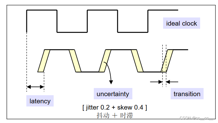
- related constraints
set_clock_uncertainty Tu [get_clocks CLK]   # clock skew + jitter
set_clock_latency -source 3 CLK
set_propagated_clock CLK
-
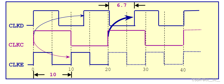
Multiple clocks (synchronous)
※综合多个约束条件进行综合。
-
Multiple clocks (asynchronous)
# use for constraining asynchronous paths or logically false paths
set_false_path -from [get_clocks CLKA] -to [get_clocks CLKB]
- Multi-cycle behavior
① Add pipeline stage(s) to divide the logic into single-cycle paths
② Ease off the single-cycle requirement: allow more clock cycles
# The default hold check is one edge before the setup
set_multicycle_path 2 -from [get_cells FF1] -to [get_cells FF2]
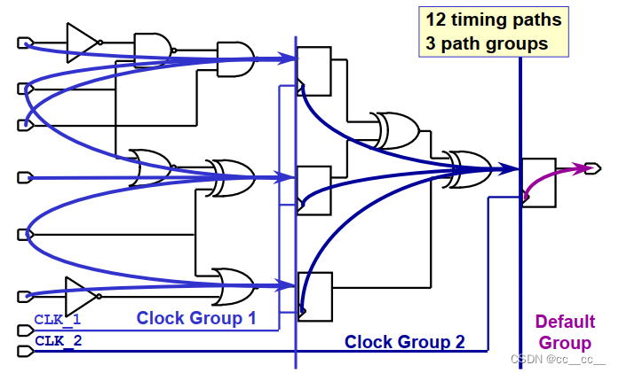
⭐时序分析
- Design is broken down into sets of timing paths.
※ start point: 1) input ports; 2) clock pins of FFs or registers.
※ end point: 1) output ports; 2) data inputs pins of sequential devices.
⭐优化策略
1. Architecture-Level optimization (HLS)
① DesignWare Implementation Selection: set_synthetic_library “dw_foundation.sldb”
② Sharing Common Sub-expressions
③ Resource Sharing
④ Reordering Operators
2. Logic-Level optimization
①Structure: set_structure true | false
②flatten: set_flatten true -effort low | medium | high
3. Gate-Level optimization
Combinational and Sequential Mapping
⭐编译策略
compile -map_effort (low | medium | high)
compile -incremental_mapping
# fix hold violation
set_fix_hold [all_clocks]
compile -only_design_rule


 3431
3431

 被折叠的 条评论
为什么被折叠?
被折叠的 条评论
为什么被折叠?
 到【灌水乐园】发言


