硬件开发——LPDDR5x

硬件开发——LPDDR5x

小狼@http://blog.youkuaiyun.com/xiaolangyangyang


1、LPDDR5(x)命令

  • DES:deselect
  • NOP:no operation
  • PDE:power down entry
  • ACT-1:activate-1
  • ACT-2:activate-2
  • PRE:precharg
  • REF:refresh
  • MWR:mask write
  • WR:write
  • WR32:write32
  • RD:read
  • RD32:read32
  • CAS:WCK到CK时钟对齐
  • MPC:multi purpose command
  • SRE:self refresh entry
  • SRX:self refresh exit
  • MRW-1:mode register write-1
  • MRW-2:mode register write-2
  • MRR:mode register read
  • WFF:write fifo
  • RFF:read fifo
  • RDC:read DQ calibration


        从DDR5开始,地址线总线与命令总线混合编码,ACT指令带有bank地址和row地址,WR/WR32/RD/RD32指令带有column地址。

2、DDR结构

3、模式寄存器

DDR3有4个MR寄存器,DDR5有256个MR寄存器。
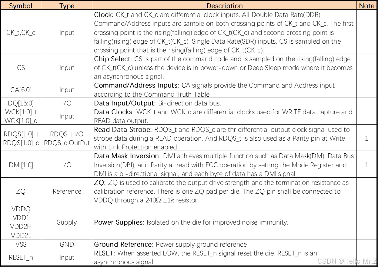
DDR5 SDRAM中模式寄存器分配和定义

4、LPDDR5(x)芯片引脚定义

5、DDR4/DDR5内存条引脚定义

6、DFI5.1信号定义

7、Training

  • CA Training:
  • CS Training:
  • Write leveling:PCB采用Fly-By拓扑结构时,控制信号与数据信号线长不一致(一般控制信号新更长),用于调整控制信号延时,方法是写DRAM寄存器使其进入training模式(此时DRAM会将CK信号作为数据返回给host),host发出CK和控制信号,读取接收数据是否为1(DRAM回复的CK高电平),如果不是说明控制信号高电平时,CK还未回复,加大CK延时继续测试,直到收到数据为1。涉及到的延时包括tDQSS/tDSS/tDSH/tWLMRD/tWLO/tWLOE。
  • VrefCA Training:
  • VrefCS Training:
  • VrefDQS Training:

8、延时参数

  • Xilinx PS使用DDR4需配置的延时参数:tCL/tRCD/tRP/tCWL/tRC/tRAS/tFAW/tAL
  • DDR5 write leveling涉及的延时参数:tDQSS/tDSS/tDSH/tWLMRD/tWLO/tWLOE
  • Uboot DDR驱动需配置的延时参数:
    tREF:内存刷新周期
    tCL:CAS延时
    tDQSS:写入DQS时间
    tMRD:模式寄存器命令时间
    tRAS:RAS到预充电延时
    tRC:同一bank打开不同Row的最短延时
    tRCD:RAS到CAS最小延时
    tRFC:自动刷新命令时间
    tRP:预充电到RAS延时
    tRRD:不同bank打开不同Row的最短延时
    tWR:写到预充电延时
    tWTR:写到读延时
    tXP:退出下电命令时间
    tXSR:退出自刷新命令时间
    tESR:自刷新命令时间

9、tuning过程

        tuning过程使用ddrphy自带的控制器PMU运行tuning固件实现,分为A~K这几个过程:

(A) Bring up VDD, VDDQ, VDD2H and VAA
The first step for initializing the PHY is to apply power. The power supplies can come up and stabilize in any order. While the power supplies are coming up, all outputs will be unknown and the values of the inputs are don't cares. Once the power supplies are stable, there are rules on how the power supplies behave. See “Power Management” on page 167 for more information on the power supplies. For more information, refer to the dwc_ddrphy_phyinit_A_bringupPower() function in PhyInit documentation.

(B) Start Clocks and Reset the PHY
The second step is to start the PHY clocks and apply the synchronous reset. For more information, refer to the dwc_ddrphy_phyinit_B_startClockResetPhy() program in the provided code in the phyinit directory.

(C) Initialize PHY Configuration
The PHY supports multiple memory standards and configurations. There are configuration registers in the PHY that must be set to configure it for the correct memory type and configuration. The routine for this step details the list of configuration registers to set and how to calculate the correct values based on the system.
For more information, refer to the dwc_ddrphy_phyinit_C_initPhyConfig() function in PhyInit documentation.

(D) Load the IMEM Memory
Before the PHY training firmware can be run, the firmware program image must be loaded into the instruction memory SRAM. For more information, refer to the dwc_ddrphy_phyinit_D_loadIMEM() function in PhyInit documentation
tuning固件(ddr_phy_fw.bin)保存在memory(0x2fa00000),此处为从memory load到ddrphy的imem(ddrphy寄存器地址0x50000)里

(E) Set the PHY input clocks to the desired frequency
Set the PHY input clocks to the desired operating frequency. Before proceeding to the next step, the clock should be stable at the new frequency. For more information on clocking requirements, see ?“Clocks” on page 126. For more information, refer to the dwc_ddrphy_phyinit_E_setDfiClk() function in PhyInit documentation

(F) Write the Message Block parameters for the training firmware
For the firmware to run, it must be given some information about the system, the memory configuration, and the memory training steps that it is to run. There are several locations in the data memory that must be written for the training firmware to have these parameters. For more information, refer to the dwc_ddrphy_phyinit_F_loadDMEM() program in the provided example code for more details.

(G) Execute the Training Firmware
Step G executes device initialization plus training firmware.  Device initialization firmware (DevInit) performs the basic initialization of the PHY and DRAM that is required before any training stage is run.
Initialization includes: resetting the DRAMs;  writing the appropriate MRs;  PLL locking;  first ZQ calibration;  first LCDL calibration;  calculation of parameters to accelerate future lock operations.
There is a protocol for starting the firmware, and interacting with it to determine the training status.  For more information, refer to the dwc_ddrphy_phyinit_G_execFW() program in the provided code in the phyinit directory.
执行完成后调用dwc_ddrphy_phyinit_userCustom_G_waitFwDone()函数判断是否tuning完成

(H) Read the Message Block results
Once the training firmware has completed, it returns the results of the training in the data memory in the message block structure.  The message block can be read to obtain these results.  For more information, refer to the dwc_ddrphy_phyinit_H_readMsgBlock() program in the provided code in the phyinit directory.
使用get_mail()获取mail消息
使用decode_major_message()解析major消息
使用decode_streaming_message()解析streaming消息

(I) Load PHY Init Engine Image
Load the PHY Initialization Engine registers with the provided initialization sequence.  For more information, refer to the dwc_ddrphy_phyinit_I_loadPIEImage() program in the provided code in the phyinit directory.
tuning完成后参数已保存到ddrphy寄存器,此时可使用dwc_ddrphy_phyinit_userCustom_saveRetRegs()函数将tuning完成的参数从寄存器读出后保存到memory

(J) Initialize the PHY to Mission Mode through DFI Initialization
Initialize the PHY to mission mode by performing a DFI initialization sequence per the DFI specification

(K) PHY is ready for Mission Mode transactions
The PHY is now in mission mode.  The outputs are controlled by the DFI bus inputs and must remain valid as long as the PHY is in an operational state.  If training was run, the memory is left initialized and in the Self-Refresh state.

        在F步骤时,使用以下指定tuning过程,置1为run该过程,置0为skip该过程

ddrphy寄存器地址0x58004
SequenceCtrl[0] Run DevInit - Device/phy initialization. Should always be set.
SequenceCtrl[1] Run WrLvl - Write leveling / WCK2CK leveling
SequenceCtrl[2] Run RxEn - Read gate training
SequenceCtrl[3] Run RdDQS - read dqs training
SequenceCtrl[4] Run WrDq - write dq training
SequenceCtrl[5] RFU, must be zero
SequenceCtrl[6] Run TxDramDCA - Tx Dram duty cycle adjustment
SequenceCtrl[7] Run RxDramDCA – Phy/Dram read duty cycle adjustment
SequenceCtrl[8] RFU, must be zero
SequenceCtrl[9] Run MxRdLat - Max read latency training
SequenceCtrl[10] Run TxDFE - DRAM Tx DFE
SequenceCtrl[11] RFU, must be zero
SequenceCtrl[12] Run LPCA - CA Training
SequenceCtrl[13] Run LPCAVREF -CA Vref Training
SequenceCtrl[14] Run RxRcvr - Rx Receiver training
SequenceCtrl[15] RFU, must be zero

        major消息包含如下,streaming消息描述了整个tuning过程,内容较多此处不作详述。

0x00: PMU Major Msg: End of DRAM offset calibration training
0x01: PMU Major Msg: End of fine write leveling
0x02: PMU Major Msg: End of read enable training
0x03: PMU Major Msg: End of read delay center optimization
0x04: PMU Major Msg: End of write delay center optimization
0x05: PMU Major Msg: End of Rx Strobeless Mode
0x06: PMU Major Msg: End of Tx DRAM DCA training
0x07: PMU Major Msg: Training has run successfully(firmware complete)
0x08: PMU Major Msg: Enter streaming message mode
0x09: PMU Major Msg: End of MaxRdLat training
0x0a: PMU Major Msg: End of Rx DRAM DCA
0x0c: PMU Major Msg: Reserved
0x0d: PMU Major Msg: End of CA training
0x0e: PMU Major Msg: End of TxDFE training
0x0f: PMU Major Msg: Reserved
0x14: PMU Major Msg: End of Rx Receiver-Vref offset training
0xfd: PMU Major Msg: End of Read Training center optimization(SI Friendly portion of 1d RdDqs training)
0xfe: PMU Major Msg: End of Write leveling(Coarse)
0xff: PMU Major Msg: Training has failed(firmware complete)
default: PMU Major Msg: Un-recongmized message

        pstate定义(power state):ddrphy支持4种pstate,pstate0/pstate1/pstate2/pstate3,包含4组影子寄存器,不同的pstate表示不同的ddr运行频率和电压,用以实现dvfs。

方案1:单独tuning 1种pstate,如下:
8533/6400/4800/3200/1600/533

方案2:同时tuning 4种pstate(tuning过程是按顺序执行),然后在运行时执行dvfs,如下:
4800-3200-1600-533
8533-6400-3200-1600
8533-4800-3200-1600
8533-6400-4800-3200
...

10、问题

1、时钟(533/1600/3200/4800/6400/8533)是指什么时钟?

2、怎么知道内存条的大小信息?
        DIMM内存条有SPD(Serial Presence Detect)芯片,一般使用I2C/I3C协议,保存有容量、厂商、频率、ECC校验等信息。DDR5上还有PMIC芯片,用于电源管理。


[持续演进]资料整理:可以学习 N 小时的 DDR

LPDDR5/5X 协议解读(一)
LPDDR5/5X 协议解读(二)Clocking
LPDDR5/5X 协议解读(三)WCK operation
LPDDR5/5X 协议解读(四)Row operation
LPDDR5/5X 协议解读(五)Read operation
LPDDR5/5X 协议解读(六)Write operation
LPDDR5/5X 协议解读(七)Refresh operation
LPDDR5/5X 协议解读(八)Power Down operation
LPDDR5/5X 协议解读(九)MR operation

DDR自学整理1---DDR3上电初始化
DDR自学整理2---DDR模式寄存器
DDR自学整理3---DDR时钟切换
DDR自学整理4---DDR write leveling
DDR自学整理5---DDR 命令
DDR自学整理6---终端电阻ODT
DDR自学整理7---ZQ Calibration
DDR自学整理8--DDR timing 名词速查手册(不定时增补)
DDR自学整理9-- DDR 状态机进一步分析
DDR自学整理10--DFI 接口
DDR自学整理11--DFI 时序
DDR自学整理12--DDR 自刷新(self-refresh)
DDR自学整理13--DDR timing 分析1
DDR自学整理14--DDR timing 分析2
DDR自学整理15--DDR DFI-DBI特性
DDR自学整理16--DDR truth table

判决反馈均衡(DFE)在DDR5中的应用

DDR 学习时间 (Part A - 1):一篇 2002 年的 DDR 控制器设计硕士论文
DDR 学习时间 (Part A - 2):学习 Micron DDR4 TN-40-07: DDR4 功耗估算 (1)
DDR 学习时间 (Part A - 2):学习 Micron DDR4 TN-40-07: DDR4 功耗估算 (2) 完
DDR 学习时间 (Part A - 3):翻译 Micron DDR TN-46-15: 低功耗与标准 DDR SDRAM 对比
DDR 学习时间 (Part B - 1):DRAM 刷新
DDR 学习时间 (Part B - 2):DRAM 自刷新
DDR 学习时间 (Part B - 3):Write Leveling
DDR 学习时间 (Part B - 4):DRAM 上电与复位初始化
DDR 学习时间 (Part B - 5):DRAM 颗粒容量规格
DDR 学习时间 (Part B - 6):DRAM ZQ 校正
DDR 学习时间 (Part C - 1):DFI 协议简介、演进和协议下载
DDR 学习时间 (Part C - 2):DFI 5.1 协议学习 目录
DDR 学习时间 (Part C - 3):DFI 协议功能 - DFI PHY 与 DFI 时钟频率比
DDR 学习时间 (Part C - 4):DFI 协议功能 - 初始化
DDR 学习时间 (Part C - 5):DFI 架构
DDR 学习时间 (Part C - 6):DFI 协议功能-写传输
DDR 学习时间 (Part C - 9):DFI 协议功能- LPDDR4 多通道模式
DDR 学习时间 (Part D - 1):[TL]DDR调试与兼容性验证系列讲座(一)
DDR 学习时间 (Part D - 2):[TL]DDR调试与兼容性验证系列讲座(二)
DDR 学习时间 (Part I - OS1):DDR IP 开源实现 DDR5 PHY 数据通路
DDR 学习时间 (Part I - OS2):DDR 开源实现 高云 GW2A FPGA 的 DDR3 低延迟控制器
DDR 学习时间 (Part M - 2):Synopsys DDR 相关技术白皮书与 IP 技术公告合集
DDR 学习时间 (Part S - 1):运行 Micron DDR3 仿真模型
DDR 学习时间 (Part Z - 1):芯片设计中的 DDR 模型杂谈

uboot-step 8 内存初始化
uboot源码学习(8)DDR内存时序参数
DDR5看这一篇就够了-硬件篇

评论
添加红包

请填写红包祝福语或标题

红包个数最小为10个

红包金额最低5元

当前余额3.43前往充值 >
需支付:10.00
成就一亿技术人!
领取后你会自动成为博主和红包主的粉丝 规则
hope_wisdom
发出的红包
实付
使用余额支付
点击重新获取
扫码支付
钱包余额 0

抵扣说明:

1.余额是钱包充值的虚拟货币,按照1:1的比例进行支付金额的抵扣。
2.余额无法直接购买下载,可以购买VIP、付费专栏及课程。

余额充值