


 这篇博客汇总了运放电路中电容的各种特殊用途,包括:提供高频小信号的负反馈,滤除电源中的交流成分,实现相位补偿和消振,防止高频自激,以及作为低通滤波器。电容在运放电路中的应用涉及到稳定系统、噪声管理和频率响应调整。
最近在进行实验室项目PCB设计的时候,看到一些运放电路中总有一些电容,但是由于自己非电子专业科班出身,对于这些电容的用法不是很懂。
于是就自己上网搜集资料,先总结如下,方便将来回顾。

1.https://zhidao.baidu.com/question/390123272773618365.html
回答1:
- 1、C1和R1组成具有一定频率特性的负反馈电路,如果没有C1,那么电路的频率特性是平直的,并联C1后,频带高端的负反馈增大,同时,也可以抑制高频自激。
2、R2和R4是运放同相端的静态偏置电路,C2是为了滤除正负1.5V电源中的残余交流成分,使偏置电压更平稳。
回答2:
- 电容器的作用是同交流隔离直流。
R1阻值太大,小的交流信号不能通过,并联一个C1就是提供一个高频小信号的负反馈电路。用于消除运放内部半导体结电容等引起的自激。
回答3:
- 消振作用和相位补偿
2.https://zhidao.baidu.com/question/494192495.html
运算放大器 积分电路 正相输入端接地 输入电压vi经电阻接 反相输入端, 电容一段接反相输入端 一端接输出v0 有一电阻和电容并联 此电路是什么作用?
回答:
- 理想积分器是不用并联这个电阻的。
实际的积分器由于运算放大器难免会存在偏置电压,尽管偏置电压很低,还是会对电容进行充放电,时间一长,电容就饱和了(充电到正电源或负电源电压)。并联电阻的目的就是为了使给电容提供放电回路,不要饱和。
并联电阻后的积分器的传递函数已经不是理想积分器了,但是,只要输入信号周期远远大于RC常数,可以近似为积分器。
3.https://www.amobbs.com/thread-5683381-1-1.html

回答:
- 输出端的高频信号有一部分会通过C返回到输入端。 不过返回来的信号跟输入的信号相位相反。 所以会有一部分高频信号被抵消掉了。
最后反映到输出端的现象就是低频增益变大。 即低通滤波
4.http://blog.sina.com.cn/s/blog_b526d0f10102yl13.html
回答:
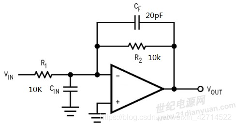
- CF的作用:相位补偿,防止振荡,抑制高频噪声。 Why?
一般来说,因为布线的寄生电容,使得运放的输入端都会有一个10~20pF的寄生电容,如图CIN(我们暂且将它称为输入电容)。正是这个输入电容,会使得运放的高频噪声增益很大,从而有可能使系统不稳定。
我们的输入信号一般为直流信号或低频信号,这个电容此时不会起作用,因而此时的增益为-R2/R1。
引发系统不稳定的是高频噪声,所以我们可以暂且抛开信号增益,只讨论电路的噪声增益。该网络的反馈系数是R1/(R1+R2),因而噪声增益为(R1+R2)/R1
(这里我也不是很明白,欢迎大伙补充说明)。
当噪声的频率比较高的时候,则需要考虑输入电容CIN对噪声增益的贡献,对于高频噪声来说,R1与CIN为并联关系,因而此时的噪声增益为:[R2+(R1//1/ωCIN)]/(R1//1/ωCIN)。
从这个噪声公式可以看出,当噪声频率越高,噪声增益公式的分母越小,噪声增益的值就越大(是不是感觉像是伯德图中零点的作用?),系统就越不容易稳定。
How?
引入CF滞后,噪声增益公式变为:[(R2//1/ωCF)+(R1//1/ωCIN)]/(R1//1/ωCIN),当频率ω增大,噪声增益公式中分母减小的同时,分子也在减小,因而噪声增益公式整体就不会随着1/ω的增大而增大。如果从伯德图看来,这里是引入了一个极点。
一般要求是R1 X CIN 大于等于 R2 X CF。
5.https://www.zhihu.com/question/46175336/answer/1053498177
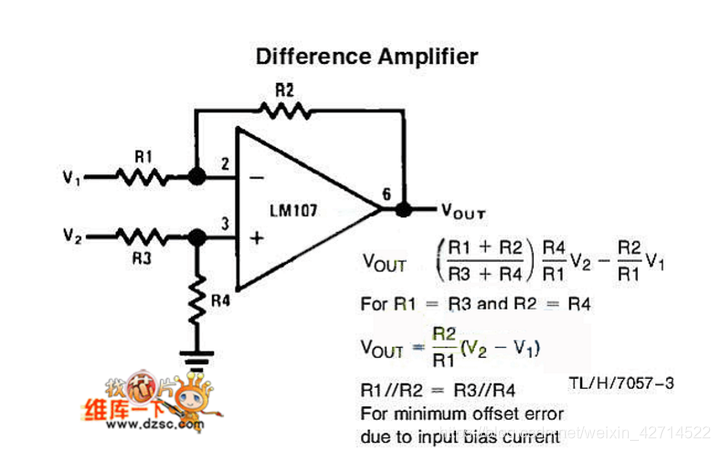
先说结论,这个电容的目的应该是降低系统的高频增益。防止系统出现高频自激振荡之类的问题。其实图中已经推导了系统的传递函数为 那么在R2和R4上增加的电容实际上就是改变了电阻R2和R4两端的阻抗而已,所以新的传递函数为(假定两个电容容值都是C) 所以系统引入一个新的极点。合理配置该极点就能够使得系统的幅值裕度增加,避免出现自激振荡。
作者:其遇
链接:https://www.zhihu.com/question/46175336/answer/1053498177
来源:知乎
著作权归作者所有。商业转载请联系作者获得授权,非商业转载请注明出处。
5.https://www.sciencedirect.com/topics/engineering/feedback-capacitor
-
Introduction to Spice Noise Analysis Art Kay, in Operational
Amplifier Noise, 20124.5 Feedback Capacitor Simulation Example A common op-amp circuit uses a feedback capacitor to limit the bandwidth. Limiting op-amp
bandwidth will reduce noise, so a feedback capacitor is a common way
to reduce noise. To understand how the feedback capacitor works,
consider that a capacitor acts as a short to “high frequency” AC
signals. Thus, at high frequencies the capacitor will short out the
feedback resistor. When the feedback resistor is shorted, the noise
gain will reduce gain to unity.In the circuit shown in Figure 4.26, the DC noise gain is 11. The
gain begins to roll off at the pole fp=1/(2πC1Rf). As the capacitive
reactance decreases, the gain decreases to unity. At higher frequency
the gain begins to decrease because of the op-amp gain bandwidth
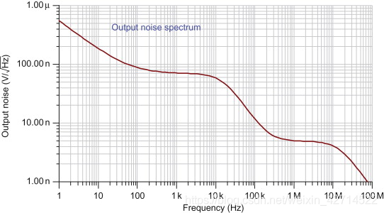
limitation. Figure 4.27 shows the noise gain transfer function and
Figure 4.28 shows the output spectral density curve. Figure 4.29
shows the total RMS noise. Note that the region where the noise gain
is unity contributes to the total noise. This region can be
eliminated using an external filter (see Figure 4.30).
Sign in to download full-size image Figure 4.26. Feedback capacitor
simulation example circuit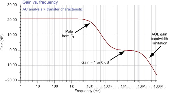
Sign in to download full-size image Figure 4.27. Noise gain vs.
frequency for Figure 4.26
Sign in to download full-size image Figure 4.28. Output noise
spectral density for Figure 4.26
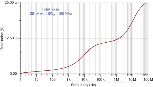
Sign in to download full-size image Figure 4.29. Total noise for
Figure 4.26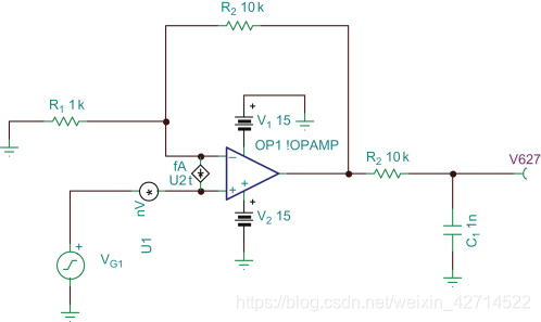
Sign in to download full-size image Figure 4.30. External filter
simulation example circuitFigure 4.30 shows an op-amp circuit with a filter at the output. This
circuit has an advantage over the feedback capacitor filter because
the external filter does not have the region where the noise gain is
limited to unity. Figure 4.31 compares the two filtering techniques.
Note that the external filter continues to attenuate but the Cf
filter attenuation stops attenuating when the gain is one (0 dB).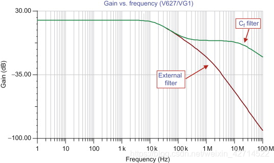
Sign in to download full-size image Figure 4.31. Noise gain vs.
frequency for different filtersFigure 4.32 shows the noise spectral density of both filter types.
From Figure 4.33, you can see that the external filter is more
effective at reducing noise. The feedback capacitance filter is most
effective on amplifiers with high gain. Remember that the feedback
capacitance will reduce the gain to unity at high frequency. The
external filter is effective regardless of the gain; however, it
increases the output impedance. The external filter is useful when
the next stage is high impedance.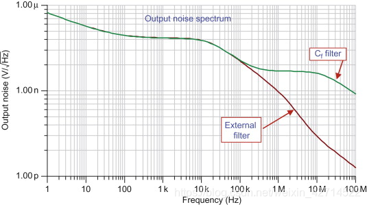
Sign in to download full-size image Figure 4.32. Spectral density for
different filters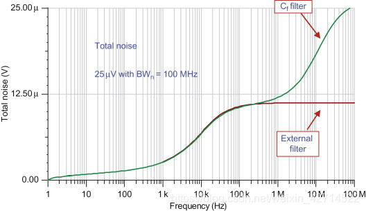
Sign in to download full-size image Figure 4.33. Total noise for
different filters


 147
147

 被折叠的 条评论
为什么被折叠?
被折叠的 条评论
为什么被折叠?
 到【灌水乐园】发言


