


 本文详细介绍了从规格制定到最终布局验证的ASIC设计全流程,包括RTL级编码、DFT内存自测、动态仿真验证、设计环境配置、综合与时序分析、布局布线、静态时序分析及功能验证等关键步骤。
|
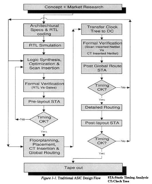
1. Architectural and electrical specification. 2. RTL(Register Transfer Level) coding in HDL(Hardware Description Language). 3. DFT(Design For Test) memory BIST(Built In Self Test) insertion, for designs containing memory elements. 4. Exhaustive dynamic simulation of the design, in order to verify the functionality of the design. 5. Design environment setting. This includes the technology library to be used, along with other environmental attributes. 6. Constraining and synthesizing the design with scan insertion (and optional JTAG) using Design Compiler. 7. Block level static timing analysis, using Design Compiler’s built-in static timing analysis engine. 8. Formal verification of the design. RTL compared against the synthesized netlist, using Formality. 9. Pre-layout static timing analysis on the full design through PrimeTime. 10. Forward annotation of timing constraints to the layout tool. 11. Initial floorplanning with timing driven placement of cells, clock tree insertion and global routing 12. Transfer of clock tree to the original design (netlist) residing in Design Compiler. 13. In-place optimization of the design in Design Compiler. 14. Formal verification between the synthesized netlist and clock tree inserted netlist, using Formality. 15. Extraction of estimated timing delays from the layout after the global routing step (step 11). 16. Back annotation of estimated timing data from the global routed design, to PrimeTime. 17. Static timing analysis in PrimeTime, using the estimated delays extracted after performing global route. 18. Detailed routing of the design. 19. Extraction of real timing delays from the detailed routed design. 20. Back annotation of the real extracted timing data to PrimeTime. 21. Post-layout static timing analysis using PrimeTime. 22. Functional gate-level simulation of the design with post-layout timing (if desired). 23. Tape out after LVS(Layout Versus Schematic) and DRC(Design Rule Checking) verification.
|


 176
176

 被折叠的 条评论
为什么被折叠?
被折叠的 条评论
为什么被折叠?
 到【灌水乐园】发言


