


注:机翻,未校。
The Rise, Fall and Revival of AMD
By Nick Evanson and Graham Singer June 29, 2020
AMD is one of the oldest designers of large scale microprocessors and has been the subject of polarizing debate among technology enthusiasts for nearly 50 years. Its story makes for a thrilling tale – filled with heroic successes, foolhardy errors, and a close shave with rack and ruin. Where other semiconductor firms have come and gone, AMD has weathered many storms and fought numerous battles, in boardrooms, courts, and stores.
AMD 是最古老的大规模微处理器设计商之一,近 50 年来一直是技术爱好者争论不休的主题。它的故事构成了一个惊心动魄的故事 —— 充满了英勇的成功、鲁莽的错误,以及与机架和废墟的近距离剃须。其他半导体公司来来去去,而 AMD 在会议室、法院和商店中经受住了许多风暴,打了无数场仗。
In this feature we’ll revisit the company’s past, examine the twists and turns in the path to the present, and wonder at what lies ahead for this Silicon Valley veteran.
在本专题中,我们将重温公司的过去,审视通往现在的曲折之路,并思考这位硅谷资深人士的未来。
Editor’s note: The third edition of this article was published at the end of 2022, see the most up-to-date version here.
编者按:本文的第三版于 2022 年底发布,请在此处查看最新版本。
The rise to fame and fortune 名利双收
To begin our story, we need to roll back the years and head for America and the late 1950s. Thriving after the hard years of World War II, this was the time and place to be if you wanted experience the forefront of technological innovation.
要开始我们的故事,我们需要倒退几年,前往美国和 1950 年代后期。在第二次世界大战的艰苦岁月之后蓬勃发展,如果您想体验技术创新的前沿,那么这里就是您的好去处。
Companies such as Bell Laboratories, Texas Instruments, and Fairchild Semiconductor employed the very best engineers, and churned out numerous firsts: the bipolar junction transistor, the integrated circuit, and the MOSFET (metal oxide semiconductor field effect transistor).
贝尔实验室、德州仪器和 Fairchild Semiconductor 等公司聘请了最优秀的工程师,并创造了许多第一:双极结型晶体管、集成电路和 MOSFET(金属氧化物半导体场效应晶体管)。
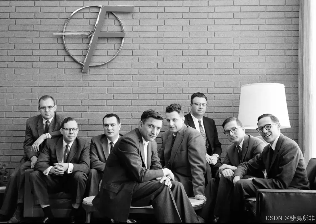
Fairchild engineers, circa 1960 – Gordon Moore is far left, Robert Noyce is in the middle foreground
Fairchild engineers ,约 1960 年 – Gordon Moore 在最左边,Robert Noyce 在中间前景
These young technicians wanted to research and develop ever more exciting products, but with cautious senior managers mindful of the times when the world was fearful and unstable, frustration amongst the engineers build a desire to strike out alone.
这些年轻的技术人员希望研究和开发更多令人兴奋的产品,但随着谨慎的高级管理人员意识到世界充满恐惧和不稳定的时代,工程师们的挫败感产生了独自出击的愿望。
And so, in 1968, two employees of Fairchild Semiconductor, Robert Noyce and Gordon Moore, left the company and forged their own path. N M Electronics opened its doors in that summer, to be renamed just weeks later as Integrated Electronics – Intel, for short.
因此,在 1968 年,Fairchild Semiconductor 的两名员工 Robert Noyce 和 Gordon Moore 离开了公司,开辟了自己的道路。NM Electronics 在那年夏天开业,几周后更名为 Integrated Electronics—— 简称 Intel。
Others followed suit and less than a year later, another 8 people left and together they set up their own electronics design and manufacturing company: Advanced Micro Devices (AMD, naturally).
其他人纷纷效仿,不到一年后,又有 8 人离开,他们一起成立了自己的电子设计和制造公司:Advanced Micro Devices(自然是 AMD)。
The group was headed by Jerry Sanders, Fairchild’s former director of marketing, They began by redesigning parts from Fairchild and National Semiconductor rather than trying to compete directly with the likes of Intel, Motorola, and IBM (who spent significant sums of money on research and development of new integrated circuits).
该小组由 Fairchild 的前营销总监 Jerry Sanders 领导,他们首先重新设计了 Fairchild 和 National Semiconductor 的零件,而不是试图与英特尔、摩托罗拉和 IBM 等公司直接竞争(他们花费了大量资金研发新的集成电路)。
From these humble beginnings, and headquartered in Silicon Valley, AMD offered products that boasted increased efficiency, stress tolerances, and speed within a few months. These microchips were designed to comply with US military quality standards, which proved a considerable advantage in the still-young computer industry, where reliability and production consistency varied greatly.
从这些不起眼的开始,总部位于硅谷的 AMD 在几个月内提供的效率、抗压能力和速度都得到提升的产品。这些微芯片的设计符合美国军用质量标准,这在仍然年轻的计算机行业中被证明是一个相当大的优势,因为该行业的可靠性和生产一致性差异很大。
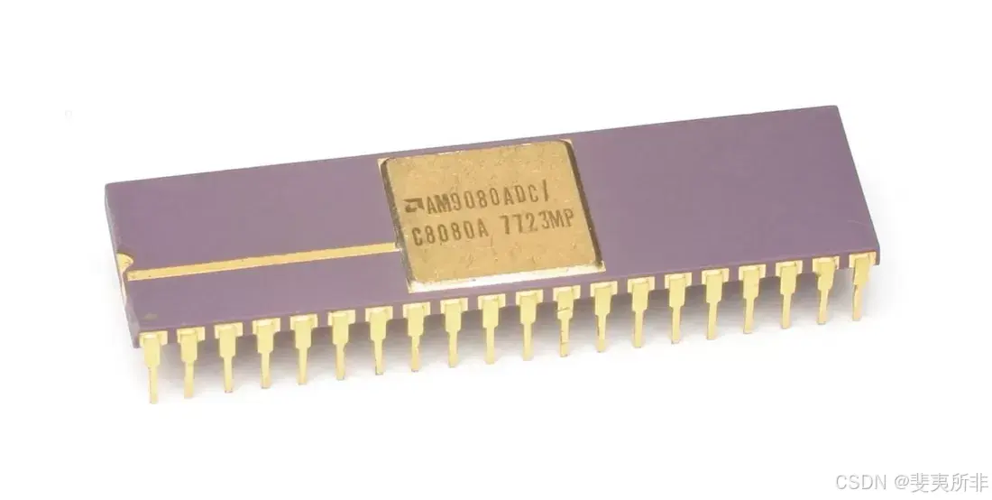
AMD’s first copycat CPU – the Am9080. Image: Wikipedia
AMD 的第一款山寨 CPU – Am9080。图片: 维基百科上的数据
By the time Intel released their first 8-bit microprocessor (the 8008) in 1974, AMD was a public company with a portfolio of over 200 products – a quarter of which were their own designs, including RAM chips, logic counters, and bit shifters. The following year saw a raft of new models: their own Am2900 integrated circuit (IC) family and the 2 MHz 8-bit Am9080, a reverse-engineered copy of Intel’s successor to the 8008. The former was a collection of components that are now fully integrated in CPUs and GPUs, but 35 years ago, arithmetic logic units and memory controllers were all separate chips.
到 Intel 于 1974 年发布他们的第一个 8 位微处理器 (8008) 时,AMD 已经是一家上市公司,拥有 200 多种产品组合,其中四分之一是他们自己的设计,包括 RAM 芯片、逻辑计数器和移位器。次年,他们推出了大量新型号:他们自己的 Am2900 集成电路 (IC) 系列和 2 MHz 8 位 Am9080,这是英特尔 8008 继任者的逆向工程副本。前者是现在完全集成在 CPU 和 GPU 中的组件集合,但在 35 年前,算术逻辑单元和内存控制器都是独立的芯片。
The blatant plagiarism of Intel’s design might seem to be somewhat shocking by today’s standards, but it was par for the course in the fledgling days of microchips.
以今天的标准来看,公然剽窃英特尔的设计似乎有些令人震惊,但在微芯片刚刚起步的时代,这已经是正常的了。
The blatant plagiarism of Intel’s design might seem to be somewhat shocking by today’s standards, but it was par for the course in the fledgling days of microchips. The CPU clone was eventually renamed as the 8080A, after AMD and Intel signed a cross-licensing agreement in 1976. You’d imagine this would cost a pretty penny or two, but it was just $325,000 ($1.65 million in today’s dollars).
以今天的标准来看,公然剽窃英特尔的设计似乎有些令人震惊,但在微芯片刚刚起步的时代,这已经是正常的了。在 AMD 和 Intel 于 8080 年签署交叉许可协议后,CPU 克隆最终更名为 1976A。您会想象这会花费一两美分,但实际上只是 325,000 美元(按今天的美元计算为 165 万美元)。
The deal allowed AMD and Intel to flood the market with ridiculously profitable chips, retailing at just over $350 or twice that for ‘military’ purchases. The 8085 (3 MHz) processor followed in 1977, and was soon joined by the 8086 (8 MHz). In 1979 also saw production begin at AMD’s Austin, Texas facility.
这笔交易使 AMD 和英特尔能够用利润丰厚的芯片充斥市场,零售价略高于 350 美元,是 “军用” 购买的两倍。8085 (3 MHz) 处理器于 1977 年推出,很快又推出了 8086 (8 MHz)。1979 年,AMD 位于德克萨斯州奥斯汀的工厂也开始生产。
When IBM began moving from mainframe systems into so-called personal computers (PCs) in 1982, the outfit decided to outsource parts rather than develop processors in-house. Intel’s 8086, the first ever x86 processor, was chosen with the express stipulation that AMD acted as a secondary source to guarantee a constant supply for IBM’s PC/AT.
当 IBM 于 1982 年开始从大型机系统转向所谓的个人计算机 (PC) 时,该公司决定将零件外包,而不是在内部开发处理器。英特尔的 8086 是有史以来第一个 x86 处理器,被选中时明确规定 AMD 作为次要来源,以保证 IBM 的 PC/AT 的持续供应。
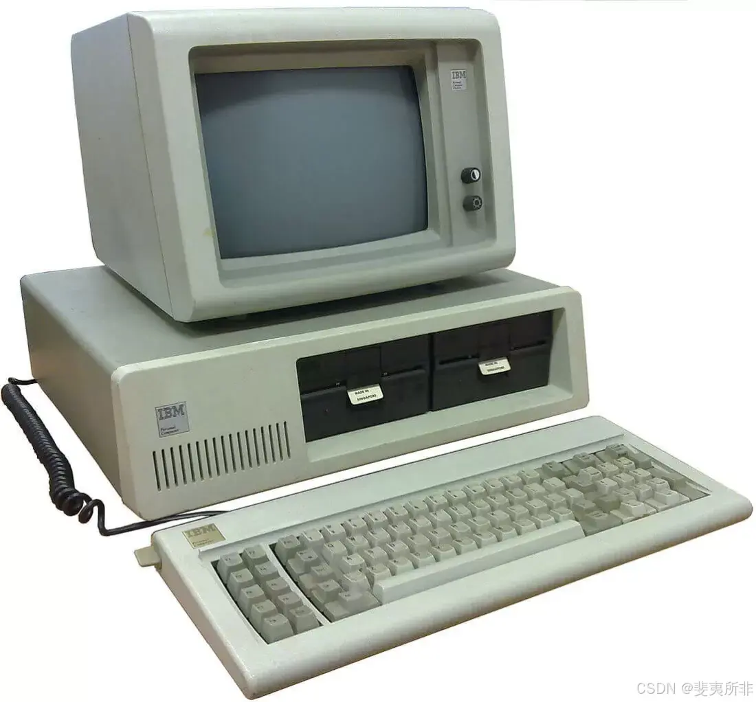
Any color, as long as it’s beige. IBM’s 5150 PC from 1981
任何颜色,只要是米色即可。1981 年的 IBM 5150 PC
A contract between AMD and Intel was signed in February of that year, with the former producing 8086, 8088, 80186, and 80188 processors – not just for IBM, but for the many IBM clones that proliferated (Compaq being just one of them). AMD also started manufacturing the 16-bit Intel 80286, badged as the Am286, towards the end of 1982.
当年 2 月,AMD 和英特尔签署了一份合同,前者生产 8086、8088、80186 和 80188 处理器 —— 不仅适用于 IBM,还用于激增的许多 IBM 克隆产品(康柏只是其中之一)。AMD 还在 16 年底开始制造 80286 位 Intel 1986,标记为 Am282。
This was to become the first truly significant desktop PC processor, and while Intel’s models generally ranged from 6 to 10 MHz, AMD’s started at 8 MHz and went as high as 20 MHz. This undoubtedly marked the start of the battle for CPU dominance between the two Silicon Valley powerhouses; what Intel designed, AMD simply tried to make better.
这将成为第一个真正重要的台式 PC 处理器,虽然 Intel 的型号通常从 6 到 10 MHz 不等,但 AMD 的型号从 8 MHz 开始,一直到 20 MHz。这无疑标志着两家硅谷强国之间争夺 CPU 主导地位的战斗的开始;Intel 设计的东西,AMD 只是想做得更好。
This period represented a huge growth of the fledgling PC market, and noting that AMD had offered the Am286 with a significant speed boost over the 80286, Intel attempted to stop AMD in its tracks. This was done by excluding them from gaining a licence for the next generation 386 processors.
这一时期代表了新兴 PC 市场的巨大增长,并注意到 AMD 为 Am286 提供了比 80286 更快的速度,英特尔试图阻止 AMD 的发展。这是通过排除他们获得下一代 386 处理器的许可证来实现的。
AMD sued, but arbitration took four and a half years to complete, and while the judgment found that Intel was not obligated to transfer every new product to AMD, it was determined that the larger chipmaker had breached an implied covenant of good faith.
AMD 提起诉讼,但仲裁花了四年半时间才完成,虽然判决认定英特尔没有义务将每款新产品都转让给 AMD,但确定这家大型芯片制造商违反了默示的诚信契约。
Intel’s licence denial occurred during a critical period, right as IBM PC’s market was ballooning from 55% to 84%. Left without access to new processor specifications, AMD took over five years to reverse-engineer the 80386 into the Am386. Once completed, it proved once more to be more than a match for Intel’s model. Where the original 386 debuted at just 12 MHz in 1985, and later managed to reach 33 MHz, the top-end version of the Am386DX launched in 1989 at 40 MHz.
英特尔的许可证被拒绝发生在一个关键时期,当时 IBM PC 的市场正从 55% 膨胀到 84%。由于无法获得新的处理器规格,AMD 花了五年多的时间将 80386 逆向工程为 Am386。一旦完成,它再次证明它与 Intel 的模型相得益彰。最初的 386 在 1985 年首次亮相时时频率仅为 12 MHz,后来成功达到 33 MHz,而 Am386DX 的高端版本于 1989 年以 40 MHz 推出。
The Am386’s success was followed by the release of 1993’s highly competitive 40 MHz Am486, which offered roughly 20% more performance than Intel’s 33 MHz i486 for the same price. This was to be replicated throughout the entire 486 line up, and while Intel’s 486DX topped out at 100 MHz, AMD offered (somewhat predictably at this stage) a snappier 120 MHz option. To better illustrate AMD’s good fortune in this period, the company’s revenue doubled from just over $1 billion in 1990 to well over $2 billion in 1994.
Am386 的成功之后,1993 年发布了极具竞争力的 40 MHz Am486,在相同的价格下,它的性能比 Intel 的 33 MHz i486 高出约 20%。这将在整个 486 系列中复制,虽然英特尔的 486DX 最高为 100 MHz,但 AMD 提供了(在这个阶段有点可以预见)更敏捷的 120 MHz 选项。为了更好地说明 AMD 在这一时期的好运气,该公司的收入从 1990 年的略高于 10 亿美元翻了一番,到 1994 年达到了 20 亿美元以上。
In 1995, AMD introduced the Am5x86 processor as a successor to the 486, offering it as a direct upgrade for older computers.
1995 年,AMD 推出了 Am5x86 处理器作为 486 的继任者,将其作为旧计算机的直接升级。
In 1995, AMD introduced the Am5x86 processor as a successor to the 486, offering it as a direct upgrade for older computers. The Am5x86 P75+ boasted a 150 Mhz frequency, with the ‘P75’ referencing performance that was similar to Intel’s Pentium 75. The ‘+’ signified that the AMD chip was slightly faster at integer math than the competition.
1995 年,AMD 推出了 Am5x86 处理器作为 486 的继任者,将其作为旧计算机的直接升级。Am5x86 P75+ 拥有 150 Mhz 的频率,“P75” 参考性能类似于 Intel 的 Pentium 75。“+” 表示 AMD 芯片在整数数学运算方面比竞争对手略快。
To counter this, Intel altered its naming conventions to distance itself from products by its rival and other vendors. The Am5x86 generated significant revenue for AMD, both from new sales and for upgrades from 486 machines. As with the Am286, 386 and 486, AMD continued to extend the market scope of the parts by offering them as embedded solutions.
为了解决这个问题,英特尔改变了其命名约定,以使其与竞争对手和其他供应商的产品保持距离。Am5x86 为 AMD 带来了可观的收入,包括新销售和 486 台机器的升级。与 Am286、386 和 486 一样,AMD 通过提供嵌入式解决方案来继续扩大这些部件的市场范围。
March 1996 saw the introduction of its first processor, developed entirely by AMD’s own engineers: the 5k86, later renamed to the K5. The chip was designed to compete with the Intel Pentium and Cyrix 6x86, and a strong execution of the project was pivotal to AMD – the chip was expected to have a much more powerful floating point unit than Cyrix’s and about equal to the Pentium 100, while the integer performance targeted the Pentium 200.
1996 年 3 月,它推出了第一款完全由 AMD 自己的工程师开发的处理器:5k86,后来更名为 K5。该芯片旨在与 Intel Pentium 和 Cyrix 6x86 竞争,该项目的强大执行对 AMD 至关重要 —— 预计该芯片将具有比 Cyrix 更强大的浮点单元,大约等于 Pentium 100,而整数性能针对 Pentium 200。
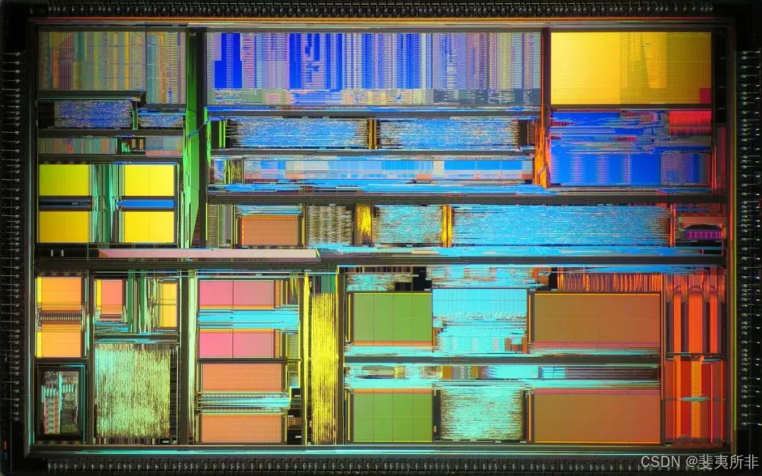
A false color image of the K5 die. Image: Wikipedia
Ultimately, it was a missed opportunity, as the project was dogged with design and manufacturing issues. These resulted in the CPU not meeting frequency and performance goals, and it arrived late to market, causing it to suffer poor sales.
最终,这是一个错失的机会,因为该项目受到设计和制造问题的困扰。这导致 CPU 无法达到频率和性能目标,并且上市时间较晚,导致销售不佳。
By this time, AMD had spent $857 million in stock on NexGen, a small fabless chip (design-only) company whose processors were made by IBM. AMD’s K5 and the developmental K6 had scaling issues at higher clock speeds (~150 MHz and above) while NexGen’s Nx686 had already demonstrated a 180 MHz core speed. After the buyout, the Nx686 became AMD’s K6 and the development of the original chip was consigned to the scrapyard.
此时,AMD 已经在 NexGen 上花费了 8.57 亿美元的股票,NexGen 是一家小型无晶圆厂芯片(仅设计)公司,其处理器由 IBM 制造。AMD 的 K5 和开发的 K6 在更高的时钟速度(~150 MHz 及以上)下存在扩展问题,而 NexGen 的 Nx686 已经展示了 180 MHz 的核心速度。买断后,Nx686 成为 AMD 的 K6,原始芯片的开发被委托给废料场。
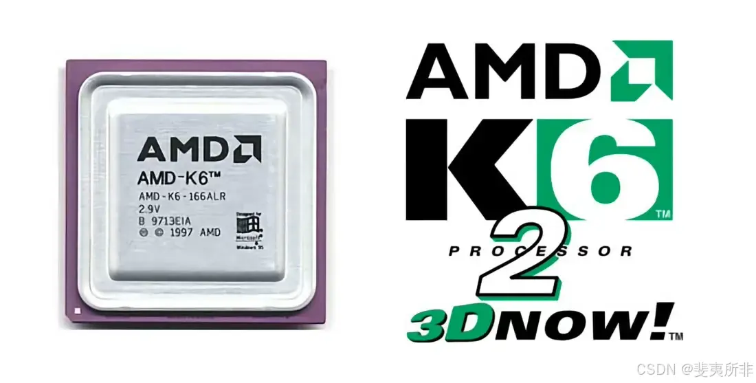
The K6-2 introduced AMD’s 3DNow! SIMD (single instruction, multiple data) instruction set.
K6-2 引入了 AMD 的 3DNow!SIMD(单指令、多数据)指令集。
AMD’s rise reflected Intel’s decline, from the early beginnings of the K6 architecture, which was pitted against Intel’s Pentium, Pentium II and (largely rebadged) Pentium III. The K6 produced a quickening of AMD’s success, owing its existence and capabilities to an ex-Intel employee, Vinod Dham (a.k.a. the “Father of Pentium”), who left Intel in 1995 to work at NexGen.
AMD 的崛起反映了英特尔的衰落,从 K6 架构的早期开始,它与英特尔的奔腾、奔腾 II 和(大部分重新贴牌的)奔腾 III 相抗衡。K6 加速了 AMD 的成功,这要归功于前英特尔员工 Vinod Dham(又名 “奔腾之父”),他于 1995 年离开英特尔前往 NexGen 工作。
When the K6 hit shelves in 1997, it represented a viable alternative to the Pentium MMX. The K6 went from strength to strength – from a 233 MHz speed in the initial stepping, to 300 MHz for the “Little Foot” revision in January 1998, 350 MHz in the “Chomper” K6-2 of May 1998, and an astonishing 550 MHz in September 1998 with the “Chomper Extended” revision.
当 K6 于 1997 年上架时,它代表了 Pentium MMX 的可行替代品。K6 不断壮大 —— 从最初步进的 233 MHz 速度,到 1998 年 1 月 “Little Foot” 修订版的 300 MHz,1998 年 5 月 “Chomper” K6-2 的 350 MHz,以及 1998 年 9 月 “Chomper Extended” 修订版的惊人 550 MHz。
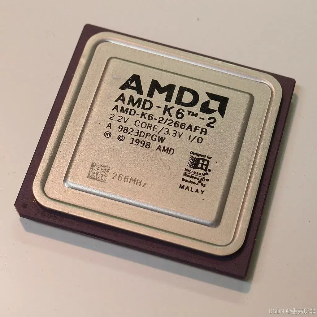
Image: Wikipedia
The K6-2 introduced AMD’s 3DNow! SIMD (single instruction, multiple data) instruction set. Essentially the same as Intel’s SSE, it offered an easier route accessing the CPU’s floating point capabilities; the downside to this being that programmers needed to incorporate the new instruction in any new code, in addition to patches and compilers needing to be rewritten to utilize the feature.
K6-2 引入了 AMD 的 3DNow!SIMD(单指令、多数据)指令集。与 Intel 的 SSE 基本相同,它提供了一条更简单的途径来访问 CPU 的浮点功能;这样做的缺点是,除了需要重写补丁和编译器才能使用该功能之外,程序员还需要将新指令合并到任何新代码中。
Like the initial K6, the K6-2 represented much better value than the competition, often costing half as much as Intel’s Pentium chips. The final iteration of the K6, the K6-III, was a more complicated CPU, and the transistor count now stood at 21.4 million – up from 8.8 million in the first K6, and 9.4 million for the K6-II.
与最初的 K6 一样,K6-2 比竞争对手的价值要高得多,其成本通常是英特尔奔腾芯片的一半。K6 的最终迭代 K6-III 是一个更复杂的 CPU,晶体管数量现在为 2140 万个,高于第一代 K6 的 880 万个和 K6-II 的 940 万个。
It incorporated AMD’s PowerNow!, which dynamically altered clock speeds according to workload. With clock speeds eventually reaching 570MHz, the K6-III was fairly expensive to produce and had a relatively short life span cut short by the arrival of the K7 which was better suited to compete with the Pentium III and beyond.
它采用了 AMD 的 PowerNow!,可根据工作负载动态改变时钟速度。随着时钟速度最终达到 570MHz,K6-III 的生产成本相当昂贵,并且相对较短的使用寿命因 K7 的到来而缩短,K7 更适合与 Pentium III 及更高版本竞争。
1999 was the zenith of AMD’s golden age – the arrival of the K7 processor, branded Athlon, showed that they were truly no longer the cheap, copycat option.
1999 年是 AMD 黄金时代的顶峰 —— 以 Athlon 为品牌的 K7 处理器的到来表明它们确实不再是廉价的山寨选择。
Starting at 500 MHz, Athlon CPUs utilized the new Slot A (EV6) and a new internal system bus licensed from DEC that operated at 200MHz, eclipsing the 133MHz Intel offered at the time. June 2000 brought the Athlon Thunderbird, a CPU cherished by many for its overclockability, which incorporated DDR RAM support and a full speed Level 2 on-die cache.
从 500 MHz 开始,Athlon CPU 使用新的插槽 A (EV6) 和从 DEC 获得许可的新内部系统总线,运行频率为 200MHz,超过了当时英特尔提供的 133MHz。2000 年 6 月推出了 Athlon Thunderbird,这是一款因其超频能力而受到许多人珍视的 CPU,它集成了 DDR RAM 支持和全速 2 级片上缓存。
2 GHz of 64-bit CPU goodness. Image: Wikipedia
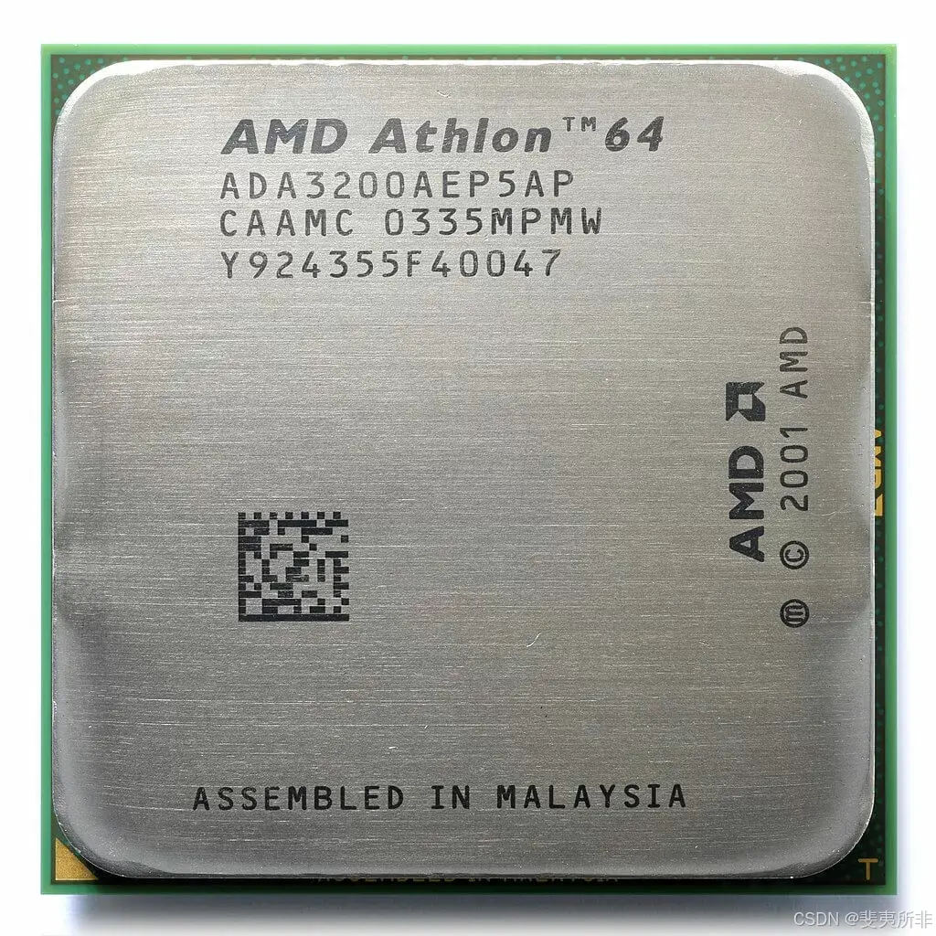
Thunderbird and its successors (Palomino, Thoroughbred, Barton, and Thorton), battled Intel’s Pentium 4 throughout the first five years of the millennium, usually at a lower price point but always with better performance. Athlon was upgraded in September 2003 with the K8 (codenamed ClawHammer), better known as the Athlon 64, because it added a 64-bit extension to the x86 instruction set.
Thunderbird 及其继任者(Palomino、Thoroughbred、Barton 和 Thorton)在千禧年的头五年与英特尔的奔腾 4 作战,通常价格较低,但性能总是更好。Athlon 于 2003 年 9 月升级为 K8(代号为 ClawHammer),更广为人知的是 Athlon 64,因为它在 x86 指令集中添加了 64 位扩展。
This episode is usually cited as AMD’s defining moment. While it was was surging ahead, the MHz-at-any-cost approach of Intel’s Netburst architecture was being exposed as a classic example of a developmental dead end.
这一事件通常被认为是 AMD 的决定性时刻。当它向前发展时,Intel 的 Netburst 架构的 MHz-ever-cost 方法被暴露为开发死胡同的典型例子。
Revenue and operating income were both excellent for such a relatively small company. While not Intel levels of income, AMD was flush with success and hungry for more. But when you’re at the very peak of the tallest of mountains, it takes every ounce of effort to stay there – otherwise, there’s only way to go.
对于这样一家相对较小的公司来说,收入和营业收入都非常出色。虽然 AMD 的收入水平低于 Intel,但 AMD 对成功充满信心,并渴望更多。但是,当您站在最高山峰的顶峰时,需要付出一切努力才能留在那里 —— 否则,只有路要走。
Paradise Lost 失乐园
There is no single event responsible for AMD tumbling from its lofty position. A global economy crisis, internal mismanagement, poor financial predictions, a victim of its own success, the fortunes and misdeeds of Intel – these all played a part, in some way or another.
没有单一的事件导致 AMD 从其崇高的位置跌落。全球经济危机、内部管理不善、糟糕的财务预测、自身成功的受害者、英特尔的财富和不当行为 —— 这些都以某种方式发挥了作用。
But let’s start seeing how matters were in early 2006. The CPU market was replete with offerings from both AMD and Intel, but the former had the likes of the exceptional K8-based Athlon 64 FX series. The FX-60 was a dual-core 2.6 GHz, whereas the FX-57 was single core, but ran at 2.8 GHz.
但是,让我们开始看看 2006 年初的情况如何。CPU 市场上充斥着 AMD 和 Intel 的产品,但前者拥有基于 K8 的卓越 Athlon 64 FX 系列。FX-60 是双核 2.6 GHz,而 FX-57 是单核,但运行频率为 2.8 GHz。
Both were head-and-shoulders above anything else, as shown by reviews at the time. They were hugely expensive, with the FX-60 retailing at over $1,000, but so was Intel’s creme-de-la-creme, the 3.46 GHz Pentium Extreme Edition 955. AMD seemed to have the upper hand in the workstation/server market as well, with Opteron chips outperforming Intel’s Xeon processors.
正如当时的评论所表明的那样,两者都比其他任何事情都高出一筹。它们非常昂贵,FX-60 的零售价超过 1,000 美元,但英特尔的精华 3.46 GHz Pentium Extreme Edition 955 也是如此。AMD 似乎在工作站 / 服务器市场也占据了上风,Opteron 芯片的性能优于 Intel 的 Xeon 处理器。
The problem for Intel was their Netburst architecture – the ultra-deep pipeline structure required very high clock speeds to be competitive, which in turn increased power consumption and heat output. The design had reached its limits and was no longer up to scratch, so Intel ditched its development and turned to their older Pentium Pro/Pentium M CPU architecture to build a successor for the Pentium 4.
Intel 的问题在于他们的 Netburst 架构 —— 超深管道结构需要非常高的时钟速度才能具有竞争力,这反过来又增加了功耗和热量输出。该设计已经达到了极限,不再符合标准,因此英特尔放弃了开发,转向他们较旧的 Pentium Pro/Pentium M CPU 架构来构建 Pentium 4 的继任者。
The initiative first produced the Yonah design for mobile platforms and then the dual-core Conroe architecture for desktops, in August 2006. Such was Intel’s need to save face that they relegated the Pentium name to low-end budget models and replaced it with Core – 13 years of brand dominance swept away in an instant.
该计划首先于 2006 年 8 月为移动平台生产了 Yonah 设计,然后为台式机生产了双核 Conroe 架构。英特尔需要挽回面子,他们将 Pentium 这个名字降级为低端预算型号,取而代之的是酷睿 ——13 年的品牌主导地位瞬间一扫而空。
The move to a low-power, high-throughput chip design wound up being ideally suited to a multitude of evolving markets and almost overnight, Intel took the performance crown in the mainstream and enthusiast sectors. By the end of 2006, AMD had been firmly pushed from the CPU summit, but it was a disastrous managerial decision that pushed them right down the slope.
向低功耗、高吞吐量芯片设计的转变最终非常适合众多不断发展的市场,几乎在一夜之间,英特尔在主流和发烧友领域夺得了性能桂冠。到 2006 年底,AMD 已经被牢牢地挤出了 CPU 峰会,但这是一个灾难性的管理决定,将他们推下了坡路。
Three days before Intel launched the Core 2 Duo, AMD made public a move that had been fully approved by then-CEO Hector Ruiz (Sanders had retired 4 years earlier). On July 24 2006, AMD announced that it intended to acquire the graphics card manufacturer ATI Technologies, in a deal worth $5.4 billion (comprising $4.3 billion in cash and loans, and $1.1 billion raised from 58 million shares). The deal was a huge financial gamble, representing 50% of AMD’s market capitalization at the time, and while the purchase made sense, the price absolutely did not.
在英特尔推出酷睿 2 双核处理器的三天前,AMD 公布了时任首席执行官赫克托・鲁伊斯 (Hector Ruiz) 完全批准的举措(桑德斯已 4 年前退休)。2006 年 7 月 24 日,AMD 宣布打算以 54 亿美元的价格收购显卡制造商 ATI Technologies(包括 43 亿美元的现金和贷款,以及从 5800 万股筹集的 11 亿美元)。这笔交易是一场巨大的金融赌博,占当时 AMD 市值的 50%,虽然收购有意义,但价格绝对没有意义。
Imageon, the handheld graphics division of ATI, was sold to Qualcomm in a paltry $65 million deal. That division is now named Adreno, an anagram of “Radeon” and an integral component of the Snapdragon SoC
ATI 的手持图形部门 Imageon 以微不足道的 6500 万美元的价格被高通公司收购。该部门现在被命名为 Adreno,这是 “Radeon” 的字谜,也是 Snapdragon SoC 的一个组成部分
ATI was grossly overvalued, as it wasn’t (nor was Nvidia) pulling in anything close to that kind of revenue. ATI had no manufacturing sites, either – it’s worth was almost entirely based on intellectual property.
ATI 被严重高估了,因为它没有(Nvidia 也没有)获得接近这种收入的任何收入。ATI 也没有制造基地 —— 它的价值几乎完全基于知识产权。
AMD eventually acknowledged this mistake when it absorbed $2.65 billion in write-downs due to overestimating ATI’s goodwill valuation.
AMD 最终承认了这一错误,由于高估了 ATI 的商誉估值,它吸收了 26.5 亿美元的减记。
To compound the lack of management foresight, Imageon, the handheld graphics division of ATI, was sold to Qualcomm in a paltry $65 million deal.That division is now named Adreno, an anagram of “Radeon” and an integral component of the Snapdragon SoC (!).
为了加剧管理层缺乏远见的情况,ATI 的手持图形部门 Imageon 以微不足道的 6500 万美元的价格被高通公司收购。该部门现在被命名为 Adreno,这是 “Radeon” 的字谜,也是 Snapdragon SoC 的组成部分 (!
Xilleon, a 32-bit SoC for Digital TV and TV cable boxes, was shipped off to Broadcom for $192.8 million.
Xilleon 是一款用于数字电视和电视有线电视盒的 32 位 SoC,以 1.928 亿美元的价格出售给博通。
In addition to burning money, AMD’s eventual response to Intel’s refreshed architecture was distinctly underwhelming. Two weeks after Core 2’s release, AMD’s President and COO, Dirk Meyer, announced the finalization of AMD’s new K10 Barcelona processor. This would be their decisive move in the server market, as it was a fully-fledged quad core CPU, whereas at the time, Intel only produced dual core Xeon chips.
除了烧钱之外,AMD 对 Intel 更新架构的最终反应显然令人印象深刻。Core 2 发布两周后,AMD 总裁兼首席运营官 Dirk Meyer 宣布 AMD 新款 K10 Barcelona 处理器的最终确定。这将是他们在服务器市场的决定性举措,因为它是一个成熟的四核 CPU,而当时英特尔只生产双核 Xeon 芯片。
The new Opteron chip appeared in September 2007, to much fanfare, but instead of stealing Intel’s thunder, the party officially halted with the discovery of a bug that in rare circumstances could result in lockups when involving nested cache writes. Rare or not, the TLB bug put a stop to AMD’s K10 production; in the meantime, a BIOS patch that cured the problem on outgoing processors, would do so at the loss of roughly 10% performance. By the time the revised ‘B3 stepping’ CPUs shipped 6 months later, the damage had been done, both for sales and reputation.
新的 Opteron 芯片于 2007 年 9 月出现,大张旗鼓,但该派对并没有抢走英特尔的风头,而是在发现一个错误后正式停止,在极少数情况下,该错误在涉及嵌套缓存写入时可能导致锁定。无论是否罕见,TLB 错误都停止了 AMD 的 K10 生产;与此同时,解决出厂处理器上问题的 BIOS 补丁将以损失大约 10% 的性能来实现。到 6 个月后修改后的 “B3 步进” CPU 发货时,销售和声誉都已经受到了损害。
A year later, near the end of 2007, AMD brought the quad-core K10 design to the desktop market. By then, Intel was forging ahead and had released the now-famous Core 2 Quad Q6600. On paper, the K10 was the superior design – all four cores were in the same die, unlike the Q6600 which used two separate dies on the same package. However, AMD was struggling to hit expected clock speeds, and the best version of the new CPU was just 2.3 GHz. That was slower, albeit by 100 MHz, than the Q6600, but it was also a little more expensive.
一年后,即 2007 年底,AMD 将四核 K10 设计引入台式机市场。那时,英特尔正在奋进,并发布了现在著名的酷睿 2 Quad Q6600。从纸面上看,K10 是卓越的设计 —— 所有四个内核都在同一个芯片中,这与 Q6600 不同,Q6600 在同一封装上使用两个单独的芯片。然而,AMD 正在努力达到预期的时钟速度,新 CPU 的最佳版本仅为 2.3 GHz。这比 Q6600 慢了 100 MHz,但也贵了一点。
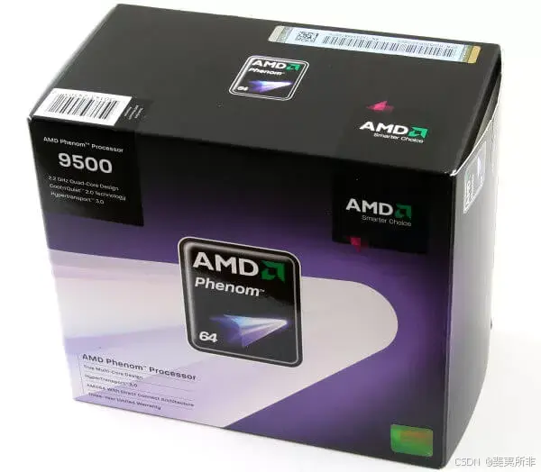
But the most puzzling aspect of it all was AMD’s decision to come out with a new model name: Phenom. Intel switched to Core because Pentium had become synonymous with excessive price and power, and having relatively poor performance. On the other hand, Athlon was a name that computing enthusiasts knew all too well and it had the speed to match its reputation. The first version of Phenom wasn’t actually bad – it just wasn’t as good as the Core 2 Quad Q6600, a product that was already readily available, plus Intel had faster offerings on the market, too.
但最令人费解的方面是 AMD 决定推出一个新型号名称:Phenom。Intel 改用 Core 是因为 Pentium 已成为价格和功率过高的代名词,并且性能相对较差。另一方面,Athlon 是计算机爱好者非常熟悉的名字,它的速度与其声誉相匹配。Phenom 的第一个版本实际上并不差 —— 它只是不如 Core 2 Quad Q6600 好,后者是一款已经很容易获得的产品,而且英特尔在市场上也有更快的产品。
Bizarrely, AMD seemed to make a conscious effort to abstain from advertising. They also had zero presence on the software side of the business; a very curious way to run a business, let alone one fighting in the semiconductor trade. But no review of this era in AMD’s history would be complete without taking into consideration Intel’s anti-competitive deeds. At this juncture, AMD was not only fighting Intel’s chips, but also the company’s monopolistic activities, which included paying OEMs large sums of money – billions in total – to actively keep AMD CPUs out of new computers.
奇怪的是,AMD 似乎有意识地努力避免投放广告。他们在业务的软件方面也为零;这是一种非常奇怪的经营方式,更不用说在半导体贸易中战斗了。但是,如果不考虑 Intel 的反竞争行为,对 AMD 历史上这个时代的回顾将是不完整的。此时,AMD 不仅与英特尔的芯片作斗争,还与该公司的垄断活动作斗争,其中包括向 OEM 支付大笔资金(总计数十亿美元),以积极将 AMD CPU 排除在新计算机之外。
In the first quarter of 2007, Intel paid Dell $723 million to remain the sole provider of its processors and chipsets – accounting for 76% of the company’s total operating income of $949 million. AMD would later win a $1.25 billion settlement in the matter, surprisingly low on the surface, but probably exacerbated by the fact that at the time of Intel’s shenanigans, AMD itself couldn’t actually supply enough CPUs to its existing customers.
2007 年第一季度,英特尔向戴尔支付了 7.23 亿美元,以保持其处理器和芯片组的唯一供应商地位,占公司总营业收入 9.49 亿美元的 76%。AMD 后来在这件事上赢得了 12.5 亿美元的和解金,表面上出奇地低,但可能由于在英特尔的恶作剧时,AMD 本身实际上无法为其现有客户提供足够的 CPU 这一事实而加剧了这种情况。
Not that Intel needed to do any of this. Unlike AMD, they had rigid long-term goal setting, as well as greater product and IP diversity. They also had cash reserves like no one else: by the end of the first decade in the new millenium, Intel was pulling in over $40 billion in revenue and $15 billion in operating income. This provided huge budgets for marketing, research and software development, as well as foundries uniquely tailored to its own products and timetable. Those factors alone ensured AMD struggled for market share.
并不是说 Intel 需要做任何这些。与 AMD 不同的是,他们有严格的长期目标设定,以及更大的产品和 IP 多样性。他们也拥有无与伦比的现金储备:到新千年的第一个十年结束时,英特尔的收入超过 400 亿美元,营业收入超过 150 亿美元。这为营销、研究和软件开发以及根据自己的产品和时间表量身定制的铸造厂提供了巨大的预算。仅这些因素就确保了 AMD 难以争夺市场份额。
A multi-billion dollar overpayment for ATI and attendant loan interest, a disappointing successor to the K8, and problematic chips arriving late to market, were all bitter pills to swallow. But matters were about to get worse.
数十亿美元的 ATI 多付和随之而来的贷款利息,令人失望的 K8 继任者,以及有问题的芯片迟到市场,都是难以下咽的苦药。但情况即将变得更糟。
One step forward, one sideways, any number back 向前一步,向侧面迈出一步,后退任意数字
By 2010, the global economy was struggling to rebound from the financial crisis of 2008. AMD had ejected its flash memory section a few years earlier, along with all its chip making foundries – they ultimately became GlobalFoundries, which AMD still uses for some of its products. Roughly 10% of its workforce had been dropped, and all together the savings and cash injection meant that AMD could knuckle down and focus entirely on processor design.
到 2010 年,全球经济正在努力从 2008 年的金融危机中反弹。几年前,AMD 推出了其闪存部门以及所有芯片制造代工厂 —— 它们最终成为 GlobalFoundries,AMD 仍在其一些产品中使用。大约 10% 的员工被裁员,节省下来的资金和现金注入意味着 AMD 可以低下头,完全专注于处理器设计。
Rather than improving the K10 design, AMD started afresh with a new structure, and towards the end of 2011, the Bulldozer architecture was launched. Where K8 and K10 were true multicore, simultaneous multithreaded (SMT) processors, the new layout was classed as being ‘clustered multithreading.’
AMD 没有改进 K10 设计,而是以新结构重新开始,并在 2011 年底推出了推土机架构。K8 和 K10 是真正的多核、同步多线程 (SMT) 处理器,而新布局被归类为 “集群多线程”。
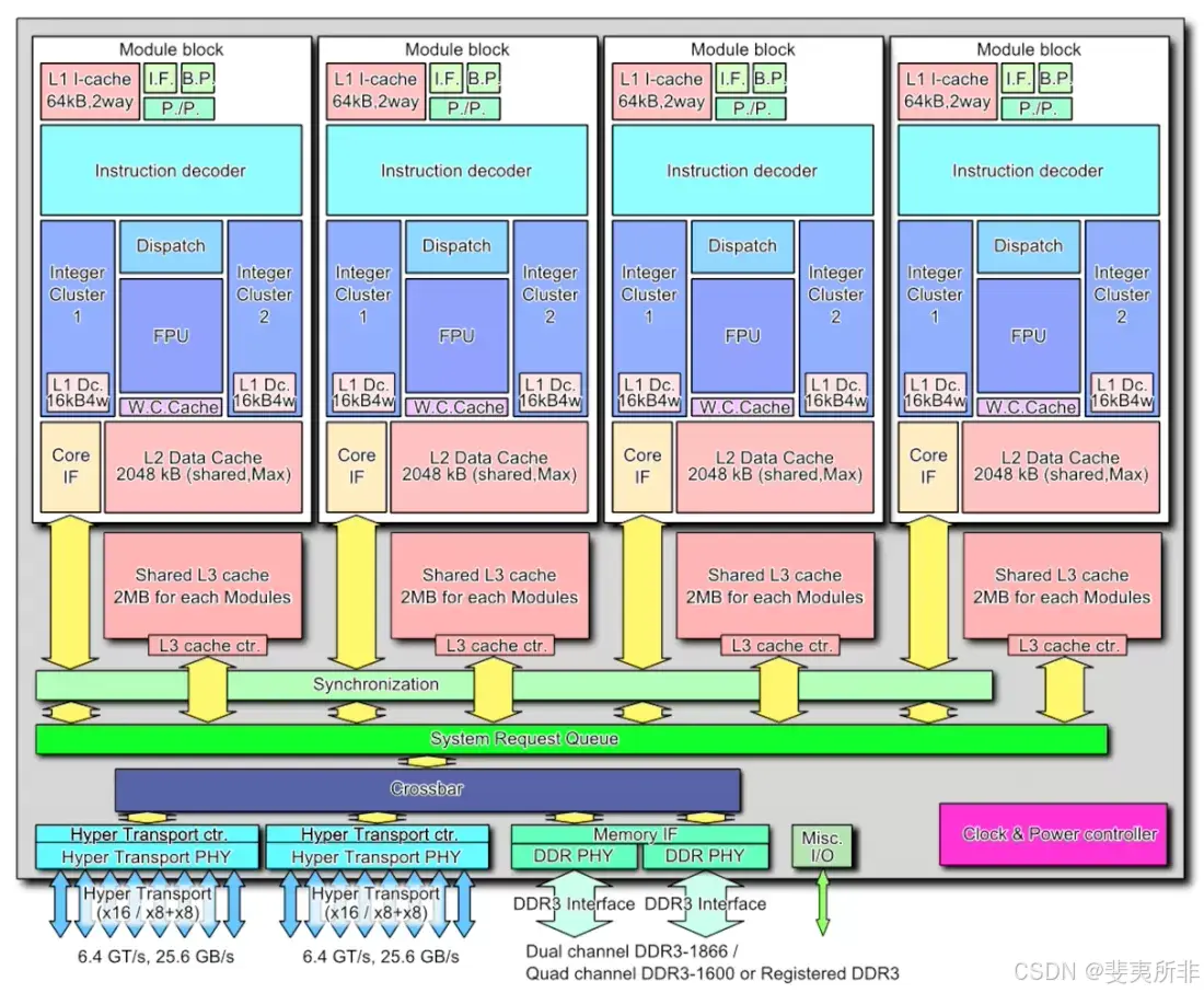
Four module design of Bulldozer. Image: [Wikipedia](https://commons.wikimedia.org/wiki/File:AMD_Bulldozer_block_diagram_(8_core_CPU).png =700x)
推土机的四模块设计。图片: 维基百科上的数据
AMD took a shared, modular approach with Bulldozer – each cluster (or module) contained two integer processing cores, but they weren’t totally independent. They shared the L1 instruction and L2 data caches, the fetch/decode, and the floating point unit. AMD even went as far as to drop the Phenom name and hark back to their glory days of the Athlon FX, by simply naming the first Bulldozer CPUs as AMD FX.
AMD 在 Bulldozer 中采用了一种共享的模块化方法 —— 每个集群(或模块)包含两个整数处理内核,但它们并不完全独立。它们共享 L1 指令和 L2 数据缓存、获取 / 解码和浮点单元。AMD 甚至放弃了 Phenom 这个名字,并通过简单地将第一批推土机 CPU 命名为 AMD FX 来回顾他们在 Athlon FX 的辉煌岁月。
The idea behind all of these changes was to reduce the overall size of the chips and make them more power efficient. Smaller dies would improve fabrication yields, leading to better margins, and the increase in efficiency would help to boost clock speeds. The scalable design would also make it suitable for a wider range of markets.
所有这些变化背后的想法是减小芯片的整体尺寸并提高它们的能效。更小的芯片将提高制造良率,从而获得更好的利润率,而效率的提高将有助于提高时钟速度。可扩展的设计也使其适用于更广泛的市场。
The best model in the October 2011 launch, the FX-8510, sported 4 clusters but was marketed as an 8 core, 8 thread CPU. By this era, processors had multiple clock speeds, and the FX-8150 base frequency was 3.6 GHz, with a turbo clock of 4.2 GHz. However, the chip was 315 square mm in size and had a peak power consumption of over 125 W. Intel had already released the Core i7-2600K: it was a traditional 4 core, 8 thread CPU, running at up to 3.8 GHz. It was significantly smaller than the new AMD chip, at 216 square mm, and used 30 W less power.
2011 年 10 月发布的最佳型号 FX-8510 具有 4 个集群,但作为 8 核、8 线程 CPU 销售。到这个时代,处理器具有多个时钟速度,FX-8150 基本频率为 3.6 GHz,睿频时钟为 4.2 GHz。然而,该芯片的尺寸为 315 平方毫米,峰值功耗超过 125 W。英特尔已经发布了酷睿 i7-2600K:它是一个传统的 4 核、8 线程 CPU,运行频率高达 3.8 GHz。它明显小于新的 AMD 芯片,为 216 平方毫米,功耗低 30 W。
On paper, the new FX should have dominated, but its performance was somewhat underwhelming – at times, the ability to handle lots of threads would shine through, but single threaded performance was often no better than the Phenom range it was set to replace, despite the superior clock speeds.
从纸面上看,新的 FX 应该占据主导地位,但它的性能有些平淡无奇 —— 有时,处理大量线程的能力会显现出来,但单线程性能通常并不比它打算取代的 Phenom 系列好,尽管时钟速度更高。
Having invested millions of dollars into Bulldozer’s R&D, AMD was certainly not going to abandon the design and the purchase of ATI was now starting to bear fruit. In the previous decade, AMD’s first foray into a combined CPU and GPU package, called Fusion, was late to market and disappointingly weak.
在投入数百万美元投入到 Bulldozer 的研发中后,AMD 肯定不会放弃这个设计,而购买 ATI 现在开始取得成果。在过去的十年中,AMD 首次涉足名为 Fusion 的 CPU 和 GPU 组合封装,上市时间较晚,而且表现不佳,令人失望。
But the project provided AMD with the means with which to tackle another markets. Earlier in 2011, another new architecture had been released, called Bobcat.
但该项目为 AMD 提供了进军另一个市场的方法。2011 年早些时候,发布了另一种名为 Bobcat 的新架构。
AMD’s custom CPU+GPU chip in the PlayStation 4. Image: Wikipedia
AMD 在 PlayStation 4 中的定制 CPU+GPU 芯片。图片: 维基百科上的数据
Aimed at low power applications, such as embedded systems, tablets, and notebooks; it was also the polar opposite design to Bulldozer: just a handful of pipelines and nothing much else. Bobcat received a much needed update a few years later, into the Jaguar architecture, and was selected by Microsoft and Sony to power the Xbox One and PlayStation 4 in 2013.
针对低功耗应用,如嵌入式系统、平板电脑和笔记本电脑;它的设计也与 Bulldozer 截然相反:只有几条管道,没有别的。几年后,山猫收到了急需的更新,进入了 Jaguar 架构,并于 2013 年被 Microsoft 和 Sony 选中为 Xbox One 和 PlayStation 4 提供支持。
Although the profit margins would be relatively slim as consoles are typically built down to the lowest possible price, both platforms sold in the millions and this highlighted AMD’s ability to create custom SoCs.
尽管由于游戏机通常以尽可能低的价格制造,因此利润率相对较低,但这两个平台的销量都达到了数百万美元,这凸显了 AMD 创建定制 SoC 的能力。
AMD’s Bobcat received an update into the Jaguar architecture, and was selected by Microsoft and Sony to power the Xbox One and PlayStation 4 in 2013.
AMD 的山猫获得了 Jaguar 架构的更新,并于 2013 年被 Microsoft 和 Sony 选中为 Xbox One 和 PlayStation 4 提供支持。
AMD continued revising the Bulldozer design over the years – Piledriver came first and gave us the FX-9550 (a 220 W, 5 GHz monstrosity), but Steamroller and the final version, Excavator (launched in 2011, with products using it 4 years later), were more focused on reducing the power consumption, rather than offering anything particularly new.
多年来,AMD 不断修改推土机的设计 —— 打桩机首先出现,给了我们 FX-9550(一个 220 W,5 GHz 的怪物),但 Steamroller 和最终版本,挖掘机(于 2011 年推出,4 年后产品使用它)更专注于降低功耗,而不是提供任何特别新的东西。
By then, the naming structure for CPUs had become confusing, to say the least. Phenom was long resigned to the history books, and FX was having a somewhat poor reputation. AMD abandoned that nomenclature and just labelled their Excavator desktop CPUs as the A-series.
至少可以说,到那时,CPU 的命名结构已经变得令人困惑。Phenom 长期以来一直被历史书所遗忘,而 FX 的声誉也有些糟糕。AMD 放弃了这个命名法,只是将他们的 Excavator 台式机 CPU 标记为 A 系列。
The graphics section of the company, fielding the Radeon products, had similarly mixed fortunes. AMD retained the ATI brand name until 2010, swapping it to their own. They also completely rewrote the GPU architecture created by ATI in late 2011, with the release of Graphics Core Next (GCN). This design would last for nearly 8 years, finding its way into consoles, desktop PCs, workstations and servers; it’s still in use today as the integrated GPU in AMD’s so-called APU processors.
该公司的图形部门负责 Radeon 产品,命运也同样喜忧参半。AMD 保留了 ATI 品牌名称直到 2010 年,并将其换成了自己的品牌。他们还在 2011 年底发布了 Graphics Core Next (GCN),完全重写了 ATI 创建的 GPU 架构。这种设计将持续近 8 年,进入游戏机、台式 PC、工作站和服务器;它今天仍然作为 AMD 所谓的 APU 处理器中的集成 GPU 使用。
Graphics Core Next’s first appearance – the Radeon HD 7970
次世代图形核心首次亮相 – Radeon HD 7970
GCN processors grew to have immense compute performance, but the structure wasn’t the easiest to get the best out of it. The most powerful version AMD ever made, the Vega 20 GPU in the Radeon VII, boasted 13.4 TFLOPs of processing power and 1024 GB/s of bandwidth – but in games, it just couldn’t reach the same heights as the best from Nvidia.
GCN 处理器逐渐具有巨大的计算性能,但这种结构并不是最容易充分利用它的结构。AMD 有史以来最强大的版本,Radeon VII 中的 Vega 20 GPU,拥有 13.4 TFLOP 的处理能力和 1024 GB/s 的带宽 —— 但在游戏中,它无法达到与 Nvidia 的最佳产品相同的高度。
Radeon products often came with a reputation for being hot, noisy, and very power hungry. The initial iteration of GCN, powering the HD 7970, required well over 200 W of power at full load – but it was manufactured on a relatively large process node, TSMC’s 28nm. By the time GCN had reached full maturity, in the form of the Vega 10, the chips were being made by GlobalFoundries on their 14nm node, but energy requirements were no better with the likes of the Radeon RX Vega 64 consuming a maximum of nearly 300 W.
Radeon 产品通常以高温、嘈杂和非常耗电而著称。为 HD 7970 供电的 GCN 的初始迭代在满载时需要超过 200 W 的功率,但它是在相对较大的工艺节点 TSMC 的 28nm 上制造的。当 GCN 以 Vega 10 的形式完全成熟时,这些芯片由 GlobalFoundries 在其 14nm 节点上制造,但能源需求并没有好到哪里去,Radeon RX Vega 64 等产品的最大功耗接近 300 W。
While AMD had decent product selection, they just weren’t as good as they should have been, and they struggled to earn enough money.
虽然 AMD 有不错的产品选择,但它们并没有达到应有的水平,而且他们很难赚到足够的钱。
| Financial Year | Revenue ($ billion) | Gross Margin | Operating Income ($ million) | Net Income ($ million) |
|---|---|---|---|---|
| 2016 | 4.27 | 23% | -372 | -497 |
| 2015 | 4.00 | 27% | -481 | -660 |
| 2014 | 5.51 | 33% | -155 | -403 |
| 2013 | 5.30 | 37% | 103 | -83 |
| 2012 | 5.42 | 23% | -1060 | -1180 |
| 2011 | 6.57 | 45% | 368 | 491 |
By the end of 2016, the company’s balance sheet had taken a loss for 4 consecutive years (2012’s financials were battered by a $700 million GlobalFoundries final write off). Debt was still high, even with the sale of its foundries and other branches, and not even the success of the system package in the Xbox and PlayStation provided enough help.
到 2016 年底,公司的资产负债表已连续 4 年亏损(2012 年的财务状况受到 7 亿美元的 GlobalFoundries 最终注销的打击)。即使出售了其铸造厂和其他分支机构,债务仍然很高,甚至 Xbox 和 PlayStation 中的系统包的成功也没有提供足够的帮助。
At face value, AMD looked to be in deep trouble.
从表面上看,AMD 似乎陷入了深深的麻烦。
New stars a-ryze 新星 a-ryze
With nothing left to sell and no sign of any large investments coming to save them, AMD could only do one thing: double-down and restructure. In 2012, they picked up two people who would come to play vital roles in the revival of the semiconductor company.
由于没有什么可出售的,也没有迹象表明任何大规模投资来拯救他们,AMD 只能做一件事:加倍下注和重组。2012 年,他们挑选了两个人,他们将在这家半导体公司的复兴中发挥重要作用。
Jim Keller, the former lead architect for the K8 range, had returned after a 13 year absence and set about heading up two projects: one an ARM-based design for the server markets, the other a standard x86 architecture, with Mike Clark (lead designer of Bulldozer) being the chief architect.
K8 系列的前首席架构师 Jim Keller 在缺席 13 年后回归,并着手领导两个项目:一个是基于 ARM 的服务器市场设计,另一个是标准 x86 架构,Mike Clark(Bulldozer 的首席设计师)是首席架构师。
Joining him was Lisa Su, who had been Senior Vice President and General Manager at Freescale Semiconductors. She took up the same position at AMD and is generally credited, along with then-President Rory Read, as being behind the company’s move into markets beyond the PC, especially consoles.
与他一起发言的是 Lisa Su,她曾担任 Freescale Semiconductors 的高级副总裁兼总经理。她在 AMD 担任过相同的职位,与当时的总裁 Rory Read 一起被普遍认为是该公司进军 PC 以外市场(尤其是游戏机)的幕后推手。
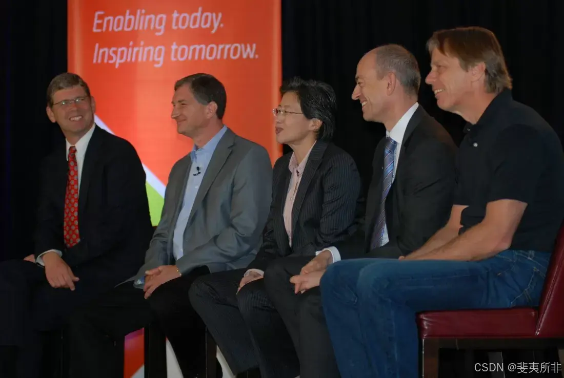
Lisa Su (middle) and Jim Keller (furthest right)
Two years after Keller’s restoration in AMD’s R&D section, CEO Rory Read stepped down and the SVP/GM moved up. With a doctorate in electronic engineering from MIT and having conducted research into SOI (silicon-on-insulator) MOSFETS, Su had the academic background and the industrial experience needed to return AMD to its glory days. But nothing happens overnight in the world of large scale processors – chip designs take several years, at best, before they are ready for market. AMD would have to ride the storm until such plans could come to fruition.
在 Keller 在 AMD 的研发部门恢复工作两年后,首席执行官 Rory Read 辞职,SVP/GM 升职。Su 拥有麻省理工学院电子工程博士学位,并从事过 SOI(绝缘体上硅)MOSFET 的研究,拥有让 AMD 重返辉煌岁月所需的学术背景和行业经验。但是,在大型处理器的世界里,没有什么是一蹴而就的 - 芯片设计充其量需要几年时间才能进入市场。AMD 将不得不乘风破浪,直到这样的计划能够实现。
While AMD continued to struggle, Intel went from strength to strength. The Core architecture and fabrication process nodes had matured nicely, and at the end of 2016, they posted a revenue of almost $60 billion. For a number of years, Intel had been following a ‘tick-tock’ approach to processor development: a ‘tick’ would be a new architecture, whereas a ‘tock’ would be a process refinement, typically in the form of a smaller node.
当 AMD 继续苦苦挣扎时,英特尔却不断发展壮大。Core 架构和制造工艺节点已经非常成熟,到 2016 年底,它们公布的收入接近 600 亿美元。多年来,英特尔一直遵循 “滴答滴答” 的处理器开发方法:“滴答滴答” 是一种新的架构,而 “滴答” 是一种流程改进,通常以较小节点的形式出现。
However, not all was well behind the scenes, despite the huge profits and near-total market dominance. In 2012, Intel expected to be releasing CPUs on a cutting-edge 10nm node within 3 years. That particular tock never happened – indeed, the clock never really ticked, either. Their first 14nm CPU, using the Broadwell architecture, appeared in 2015 and the node and fundamental design remained in place for half a decade.
然而,尽管有巨额利润和几乎完全的市场主导地位,但并非一切都在幕后进行。2012 年,英特尔预计在 3 年内在尖端 10nm 节点上发布 CPU。那个特别的 tuck 从未发生过 —— 事实上,时钟也从未真正滴答作响。他们的第一款 14nm CPU 使用 Broadwell 架构于 2015 年出现,节点和基本设计保留了五年。
The engineers at the foundries repeatedly hit yield issues with 10nm, forcing Intel to refine the older process and architecture each year. Clock speeds and power consumption climbed ever higher, but no new designs were forthcoming; an echo, perhaps, of their Netburst days. PC customers were left with frustrating choices: choose something from the powerful Core line, but pay a hefty price, or choose the weaker and cheaper FX/A-series.
代工厂的工程师反复遇到 10 纳米的良率问题,迫使英特尔每年都改进旧的工艺和架构。时钟速度和功耗攀升得越来越高,但没有新的设计出现;也许是他们 Netburst 时代的回声。PC 客户面临令人沮丧的选择:从强大的 Core 系列中选择一些东西,但要付出高昂的价格,或者选择更弱、更便宜的 FX/A 系列。
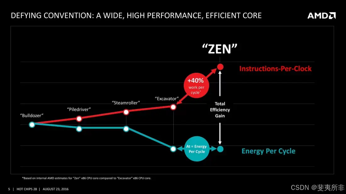
But AMD had been quietly building a winning set of cards and played their hand in February 2016, at the annual E3 event. Using the eagerly awaited Doom reboot as the announcement platform, the completely new Zen architecture was revealed to the public.
但 AMD 一直在悄悄地打造一套成功的牌,并在 2016 年 2 月的年度 E3 活动中发挥了作用。以期待已久的 Doom 重启为公告平台,全新的 Zen 架构向公众展示。
Very little was said about the fresh design besides phrases such as’simultaneous multithreading’, ‘high bandwidth cache,’ and ‘energy efficient finFET design.’ More details were given during Computex 2016, including a target of a 40% improvement over the Excavator architecture.
除了 “同步多线程”、“高带宽缓存” 和 “节能 finFET 设计” 等短语外,关于新设计的讨论很少。在 Computex 2016 期间提供了更多细节,包括比 Excavator 架构改进 40% 的目标。
To say this was ambitious would be an understatement
如果说这是雄心勃勃的,那就太轻描淡写了
To say this was ambitious would be an understatement – especially in light of the fact that AMD had delivered modest 10% increases with each revision of the Bulldozer design, at best.
说这是雄心勃勃的,那就太轻描淡写了 —— 尤其是考虑到 AMD 在推土机设计的每次修订中最多都实现了 10% 的适度增长。
It would take them another 12 months before the chip actually appeared, but when it did, AMD’s long-stewing plan was finally clear.
他们又花了 12 个月的时间才真正出现芯片,但当它出现时,AMD 的长期计划终于明确了。
Any new hardware design needs the right software to sell it, but multi-threaded CPUs were facing an uphill battle. Despite consoles sporting 8-core CPUs, most games were still perfectly fine with just 4. The main reasons were Intel’s market dominance and the design of AMD’s chip in the Xbox One and PlayStation 4. The former had released their first 6-core CPU back in 2010, but it was hugely expensive (nearly $1,100). Others rapidly appeared, but it would be another seven years before Intel offered a truly affordable hexa-core processor, the Core i5-8400, at under $200.
任何新的硬件设计都需要合适的软件来销售,但多线程 CPU 面临着一场艰苦的战斗。尽管游戏机配备 8 核 CPU,但大多数游戏仍然只使用 4 核 CPU。主要原因是英特尔的市场主导地位以及 AMD 在 Xbox One 和 PlayStation 4 中的芯片设计。前者早在 2010 年就发布了他们的第一款 6 核 CPU,但它非常昂贵(近 1,100 美元)。其他的很快就出现了,但又过了七年,英特尔才以不到 5 美元的价格提供真正实惠的六核处理器 Core i8400-200。
The issue with console processors was that the CPU layout consisted of two 4-core CPUs in the same die, and there was high latency between the two sections of the chip. So game developers tended to keep the engine’s threads located on one of the sections, and only use the other for general background processes. Only in the world of workstations and servers there was a need for seriously multi-threaded CPUs – until AMD decided otherwise.
控制台处理器的问题在于 CPU 布局由同一芯片中的两个 4 核 CPU 组成,并且芯片的两个部分之间存在很高的延迟。因此,游戏开发人员倾向于将引擎的线程位于其中一个部分,并且仅将另一个部分用于一般的后台进程。只有在工作站和服务器领域,才需要真正的多线程 CPU—— 直到 AMD 做出不同的决定。
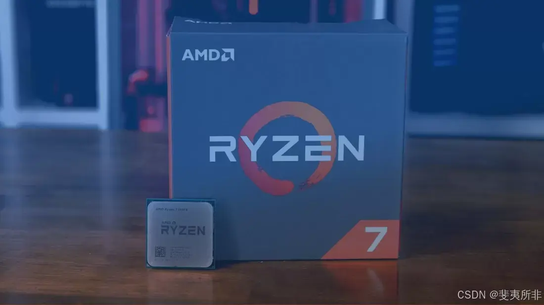
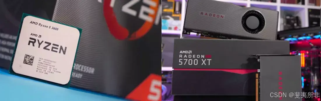
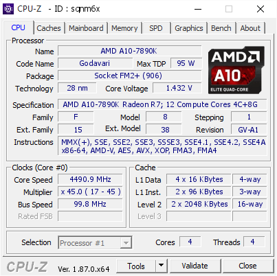
In March 2017, general desktop users could upgrade their systems with one of two 8-core,16-thread CPUs. A completely new architecture clearly deserved a new name, and AMD cast off Phenom and FX, to give us Ryzen.
2017 年 3 月,普通台式机用户可以使用两个 8 核 16 线程 CPU 之一升级他们的系统。一个全新的架构显然应该有一个新名字,AMD 抛弃了 Phenom 和 FX,给了我们 Ryzen。
Neither CPU was particularly cheap: the 3.6 GHz (4 GHz boost) Ryzen 7 1800X retailed at $500, with the 0.2 GHz slower 1700X selling for $100 less. In part, AMD was keen to stop the perception of being the budget choice, but it was mostly because Intel was charging over $1,000 for their 8-core offering, the Core i7-6900K.
这两款 CPU 都不是特别便宜:3.6 GHz(4 GHz 提升)Ryzen 7 1800X 的零售价为 500 美元,而 0.2 GHz 较慢的 1700X 的售价要低 100 美元。在某种程度上,AMD 热衷于阻止成为预算选择的看法,但这主要是因为英特尔对其 8 核产品酷睿 i7-6900K 收取超过 1,000 美元的费用。
Zen took the best from all previous designs and melded them into a structure that focused on keeping the pipelines as busy as possible; and to do this, required significant improvements to the pipeline and cache systems. The new design dropped the sharing of L1/L2 caches, as used in Bulldozer, and each core was now fully independent, with more pipelines, better branch prediction, and greater cache bandwidth.
Zen 从以前的所有设计中汲取了最好的东西,并将它们融合成一个专注于保持管道尽可能繁忙的结构;为此,需要对管道和缓存系统进行重大改进。新设计放弃了 Bulldozer 中使用的 L1/L2 缓存共享,每个内核现在都完全独立,具有更多的管道、更好的分支预测和更大的缓存带宽。
Reminiscent of the chip powering Microsoft and Sony’s consoles, the Ryzen CPU was also a system-on-a-chip
让人想起为 Microsoft 和 Sony 游戏机提供动力的芯片,Ryzen CPU 也是一种片上系统
Reminiscent of the chip powering Microsoft and Sony’s consoles, the Ryzen CPU was also a system-on-a-chip; the only thing it lacked was a GPU (later budget Ryzen models included a GCN processor).
让人想起为 Microsoft 和 Sony 游戏机提供动力的芯片,Ryzen CPU 也是一种片上系统;它唯一缺少的是 GPU(后来的廉价 Ryzen 型号包括 GCN 处理器)。
The die was sectioned into two so-called CPU Complexes (CCX), each of which were 4-core, 8-threads. Also packed into the die was a Southbridge processor – the CPU offered controllers and links for PCI Express, SATA, and USB. This meant motherboards, in theory, could be made without an SB but nearly all did, just to expand the number of possible device connections.
芯片被分成两个所谓的 CPU 复合体 (CCX),每个复合体都是 4 核、8 线程。芯片中还装有一个南桥处理器 ——CPU 为 PCI Express、SATA 和 USB 提供控制器和链接。这意味着理论上,主板可以在没有 SB 的情况下制造,但几乎所有主板都可以制造,只是为了扩大可能的设备连接数量。
All of this would be for nothing if Ryzen couldn’t perform, and AMD had a lot to prove in this area after years of playing second fiddle to Intel. The 1800X and 1700X weren’t perfect: as good than anything Intel had for professional applications, but slower in games.
如果 Ryzen 无法执行,所有这些都将是徒劳的,而 AMD 在多年仅次于英特尔之后,在这个领域还有很多东西需要证明。1800X 和 1700X 并不完美:比英特尔在专业应用程序中的任何产品都要好,但在游戏中速度较慢。
AMD had other cards to play: a month after the first Ryzen CPUs hit the market, came 6 and 4-core Ryzen 5 models, followed two months later by 4-core Ryzen 3 chips. They performed against Intel’s offerings in the same manner as their larger brothers, but they were significantly more cost effective.
AMD 还有其他牌可以打:在第一款 Ryzen CPU 上市一个月后,出现了 6 核和 4 核 Ryzen 5 型号,两个月后又推出了 4 核 Ryzen 3 芯片。它们的表现与 Intel 的产品相比,与它们的大哥相同,但它们的成本效益要高得多。
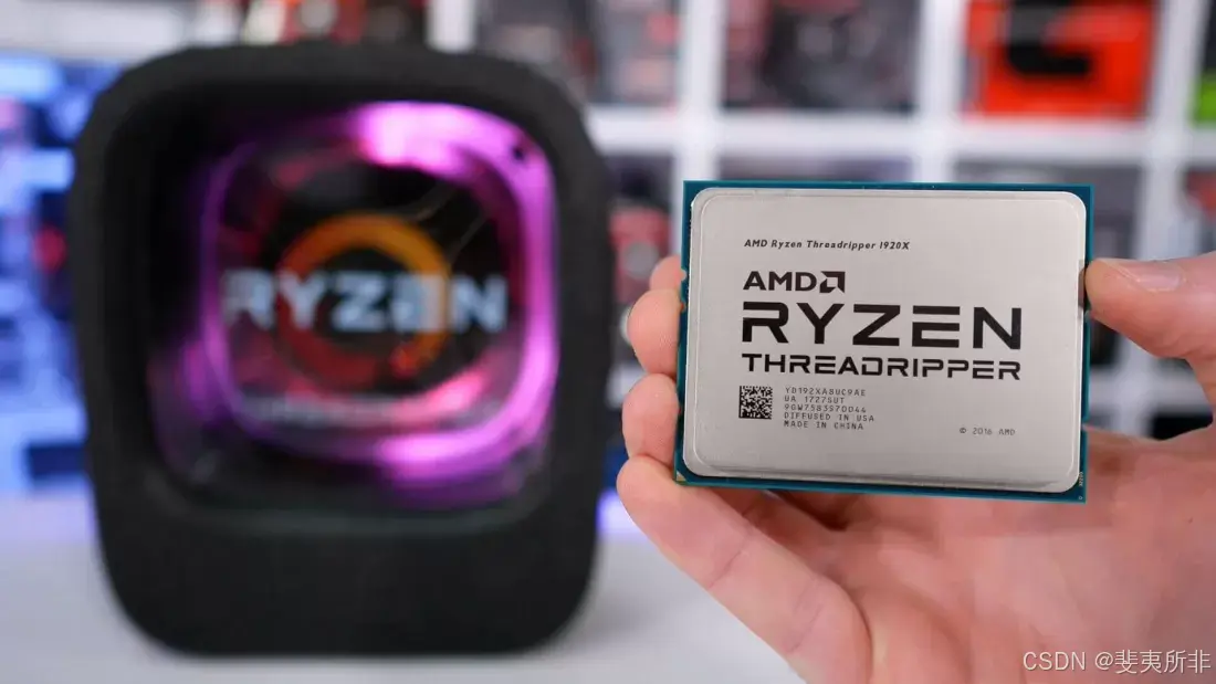
And then came the aces – the 16-core, 32-thread Ryzen Threadripper 1950X (with an asking price of $1,000) and the 32-core, 64-thread EPYC processor for servers. These behemoths comprised two and four Ryzen 7 1800X chips, respectively, in the same package, utilizing the new Infinity Fabric interconnect system to shift data between the chips.
然后是王牌 ——16 核、32 线程的 Ryzen Threadripper 1950X(要价为 1,000 美元)和用于服务器的 32 核、64 线程 EPYC 处理器。这些庞然大物分别由两个和四个 Ryzen 7 1800X 芯片组成,采用同一封装,利用新的 Infinity Fabric 互连系统在芯片之间传输数据。
In the space of six months, AMD showed that they were effectively targeting every x86 desktop market possible, with a single, one-size-fits-all design.
在六个月的时间里,AMD 表明他们通过单一、一刀切的设计有效地瞄准了每一个可能的 x86 台式机市场。
A year later, the architecture was updated to Zen+, which consisted of tweaks in the cache system and switching from GlobalFoundries’ venerable 14LPP process – a node that was under from Samsung – to an updated, denser 12LP system. The CPU dies remained the same size, but the new fabrication method allowed the processors to run at higher clock speeds.
一年后,架构更新到 Zen+,其中包括对缓存系统的调整,以及从 GlobalFoundries 古老的 14LPP 流程(三星的节点)切换到更新的、更密集的 12LP 系统。CPU 芯片的大小保持不变,但新的制造方法允许处理器以更高的时钟速度运行。
AMD launched Zen 2: this time the changes were more significant and the term chiplet became all the rage
AMD 推出 Zen 2:这一次的变化更为显着,小芯片一词风靡一时
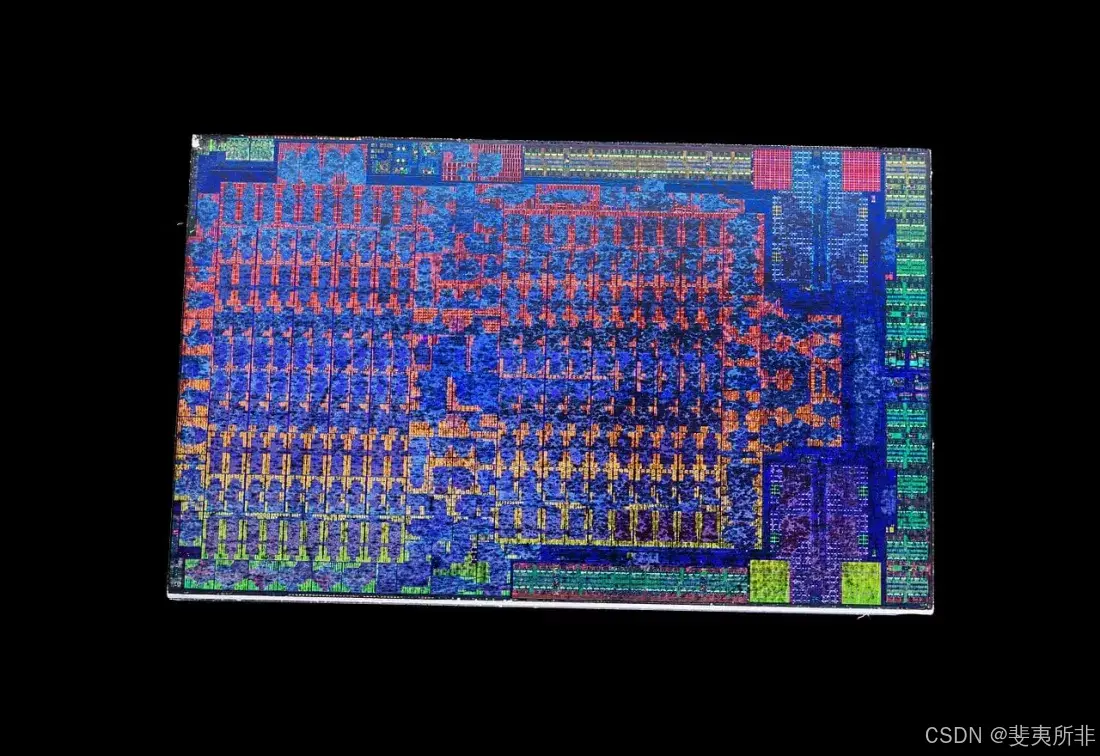
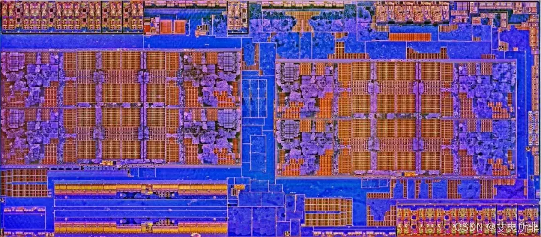
Another 12 months after that, in the summer of 2019, AMD launched Zen 2. This time the changes were more significant and the term chiplet became all the rage. Rather than following a monolithic construction, where every part of the CPU is in the same piece of silicon (which Zen and Zen+ do), the engineers separated in the Core Complexes from the interconnect system.
又过了 12 个月,即 2019 年夏天,AMD 推出了 Zen 2。这一次,变化更加显著,小芯片一词风靡一时。工程师们没有遵循 CPU 的每个部分都位于同一块硅片中的单片结构(Zen 和 Zen+ 就是这样),而是将核心复合体与互连系统分开。
The former were built by TSMC, using their N7 process, becoming full dies in their own right – hence the name, Core Complex Die (CCD). The input/output structure was made by GlobalFoundries, with desktop Ryzen models using a 12LP chip, and Threadripper & EPYC sporting larger 14 nm versions.
前者是由台积电制造的,使用他们的 N7 工艺,本身就成为全晶片 —— 因此得名 Core Complex Die (CCD)。输入 / 输出结构由 GlobalFoundries 制造,桌面 Ryzen 型号使用 12LP 芯片,而 Threadripper 和 EPYC 则具有更大的 14 nm 版本。
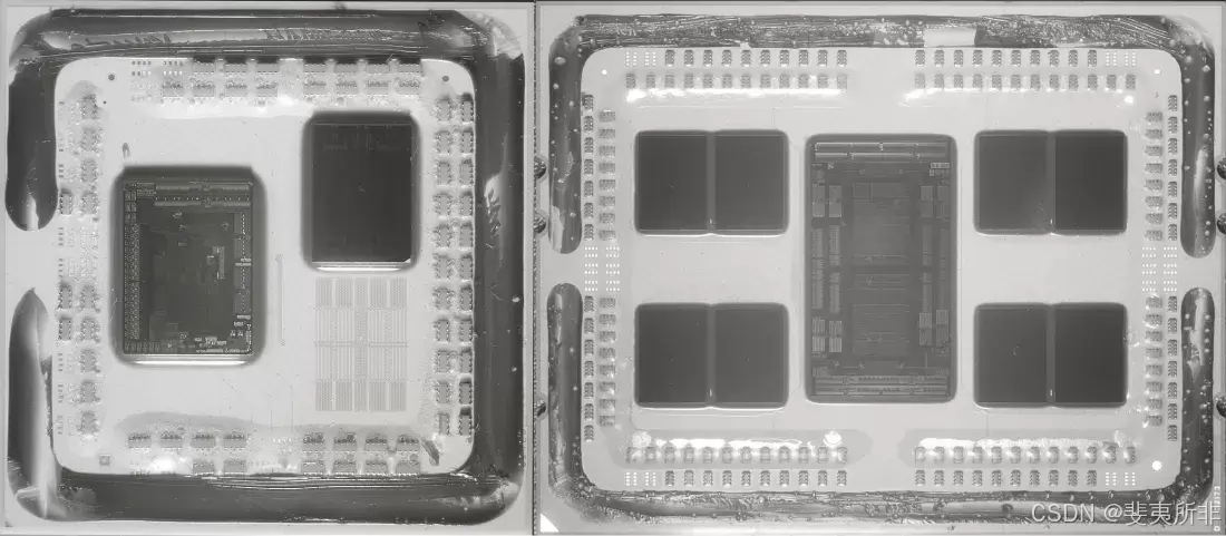
Infrared images of a Zen 2 Ryzen and EPYC. The CCD chiplets are clearly separate to the I/O chip. Image: Fritzchens Fritz
Zen 2、Ryzen 和 EPYC 的红外图像。CCD 小芯片与 I/O 芯片明显分开。图片来源: Fritzchens Fritz
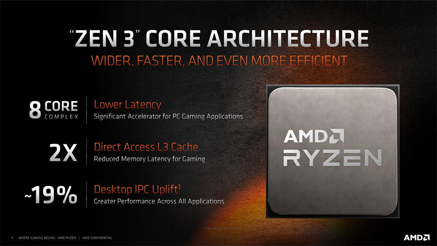
The chiplet design will be retained and refined for Zen 3, currently penned for release late in 2020. We’re not likely to see the CCDs break Zen 2’s 8-core, 16-thread layout, instead it’ll be a similar improvement as seen with Zen+ (i.e. cache, power efficiency, and clock speed improvements).
小芯片设计将在 Zen 3 中保留和改进,目前预计将于 2020 年底发布。我们不太可能看到 CCD 打破 Zen 2 的 8 核、16 线程布局,相反,它将是与 Zen+ 类似的改进(即缓存、能效和时钟速度改进)。
It’s worth taking stock with what AMD achieved with Zen. In the space of 8 years, the architecture went from a blank sheet of paper to a comprehensive portfolio of products, containing $99 4-core, 8-thread budget offerings through to $4,000+ 64-core, 128-thread server CPUs.
值得评估 AMD 通过 Zen 取得的成就。在 8 年的时间里,该架构从一张白纸变成了一个全面的产品组合,包括 99 美元的 4 核、8 线程预算产品,以及 4,000 美元的 64 核、128 线程服务器 CPU。
AMD’s finances have changed dramatically as well: from losses and debts running into the billions, AMD is now on track to clear its loans and post an operating income in excess of $600 million, within the next year. While Zen may not be the sole factor in the company’s financial revival, it has helped enormously.
AMD 的财务状况也发生了巨大变化:从数十亿美元的亏损和债务,AMD 现在有望在明年清偿贷款并实现超过 6 亿美元的营业收入。虽然 Zen 可能不是公司财务复苏的唯一因素,但它已经帮助了很大。
AMD’s graphics division has seen similar changes in fortune – in 2015, the section was given full independence, as the Radeon Technologies Group (RTG). The most significant development from their engineers came in the form of RDNA, a significant reworking of GCN. Changes to the cache structure, along with adjustments to the size and grouping of the compute units, shifted the focus of the architecture directly towards gaming.
AMD 的图形部门也经历了类似的命运变化 ——2015 年,该部门被赋予了完全独立的权利,成为 Radeon 技术集团 (RTG)。他们的工程师最重要的发展是 RDNA 的形式,这是对 GCN 的重大改造。对缓存结构的更改,以及对计算单元大小和分组的调整,将架构的重点直接转移到了游戏上。
The first models to use this new architecture, the Radeon RX 5700 series, demonstrated the design’s serious potential. This was not lost on Microsoft and Sony, as they both selected Zen 2 and the updated RDNA 2, to power their forthcoming new Xbox and PlayStation 5 consoles.
第一款使用这种新架构的型号 Radeon RX 5700 系列展示了该设计的巨大潜力。Microsoft 和 Sony 并没有忘记这一点,因为他们都选择了 Zen 2 和更新的 RDNA 2 来为他们即将推出的新 Xbox 和 PlayStation 5 游戏机提供动力。
AMD is quantifiably back to where it was in the Athlon 64 days in terms of architecture development and technological innovation. They rose to the top, fell from grace, and like a beast from mythology, created their own rebirth from the ashes.
AMD 在架构开发和技术创新方面可以量化地恢复到 Athlon 64 天的水平。他们升到顶峰,从恩典中坠落,像神话中的野兽一样,从灰烬中创造了自己的重生。
Although the Radeon Group hasn’t enjoyed the same level of success as the CPU division, and their graphics cards are perhaps still seen as the “value option,” AMD is quantifiably back to where it was in the Athlon 64 days in terms of architecture development and technological innovation. They rose to the top, fell from grace, and like a beast from mythology, created their own rebirth from the ashes.
尽管 Radeon Group 没有获得与 CPU 部门相同水平的成功,并且他们的显卡可能仍然被视为 “价值选择”,但 AMD 在架构开发和技术创新方面可以量化地恢复到 Athlon 64 天时的状态。他们升到顶峰,从恩典中坠落,像神话中的野兽一样,从灰烬中创造了自己的重生。
Looking ahead with caution 谨慎展望未来
It’s perfectly suitable to ask a simple question about AMD: could they return to the dark days of dismal products and no money?
问一个关于 AMD 的简单问题是完全合适的:他们能否回到产品惨淡、没钱的黑暗日子?
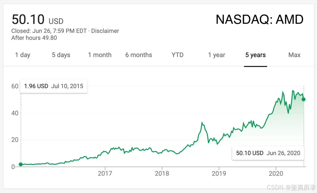
Even if 2020 proves to be an excellent year for AMD and positive Q1 financial results show a 40% improvement to the previous year, $9.4 billion of revenue still puts them behind Nvidia ($10.7 billion in 2019) and light years away from Intel ($72 billion). The latter has a much larger product portfolio, of course, and its own foundries, but Nvidia’s income is reliant almost entirely on graphics cards.
即使 2020 年对 AMD 来说是出色的一年,并且积极的第一季度财务业绩显示比上一年增长 40%,但 94 亿美元的收入仍然落后于英伟达(2019 年的 107 亿美元),与英特尔(720 亿美元)相差数光年。当然,后者拥有更大的产品组合和自己的代工厂,但 Nvidia 的收入几乎完全依赖于显卡。
AMD’s best sellers AMD 最畅销产品
It’s clear that both revenue and operating income need to grow, in order to fully stabilize AMD’s future – so how could this be achieved? The bulk of their income is from what they call the Computing and Graphics segment, i.e. Ryzen and Radeon sales. This will undoubtedly continue to improve, as Ryzen is very competitive and the RDNA 2 architecture will provide a common platform for games that work as well on PCs as they do on next-generation consoles.
很明显,收入和营业收入都需要增长,才能完全稳定 AMD 的未来 —— 那么如何实现这一目标呢?他们的大部分收入来自他们所谓的计算和图形部门,即 Ryzen 和 Radeon 的销售。这无疑将继续改进,因为 Ryzen 非常有竞争力,RDNA 2 架构将为游戏提供一个通用平台,这些游戏在 PC 上的运行效果与在下一代游戏机上一样好。
Intel’s latest desktop CPUs hold an ever decreasing lead in gaming. They also lack the breadth of features that Zen 3 will offer. Nvidia holds the GPU performance crown, but faces stiff competition in the mid-range sector from Radeons. It’s perhaps nothing more than a coincidence, but even though RTG is a fully independent division of AMD, its revenue and operating income are grouped with the CPU sector – this suggests that their graphics cards, while popular, do not sell in the same quantities as their Ryzen products do.
Intel 最新的台式机 CPU 在游戏领域的领先优势不断下降。它们也缺乏 Zen 3 将提供的广度功能。Nvidia 拥有 GPU 性能冠军,但在中端领域面临来自 Radeon 的激烈竞争。这也许只不过是一个巧合,但即使 RTG 是 AMD 的一个完全独立的部门,其收入和营业收入也与 CPU 部门归为一组 —— 这表明他们的显卡虽然受欢迎,但销量不如他们的 Ryzen 产品。
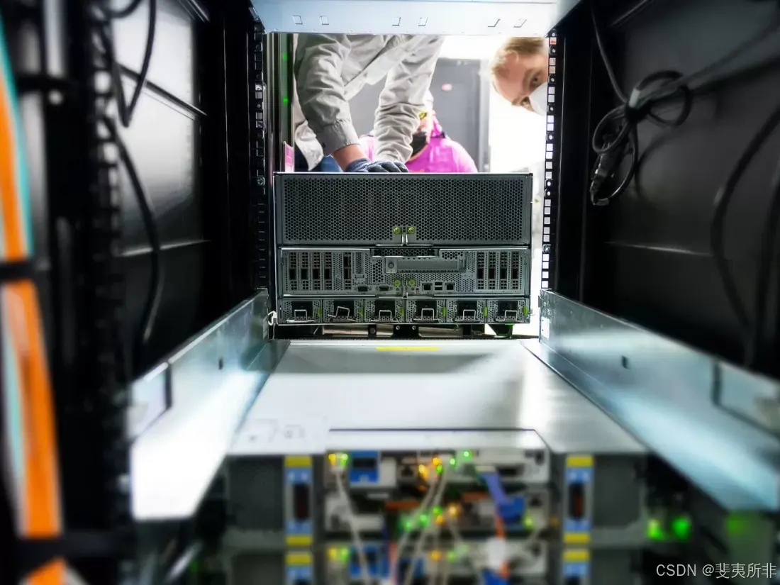
Possibly a more pressing issue for AMD is that their Enterprise, Embedded and Semi-Custom segment accounted for just under 20% of the Q1 2020 revenue, and ran at an operating loss. This may be explained by the fact that current-gen Xbox and PlayStation sales have stagnated, in light of the success of Nintendo’s Switch and forthcoming new models from Microsoft and Sony. Intel has also utterly dominated the enterprise market and nobody running a multi-million dollar datacenter is going to throw it all out, just because an amazing new CPU is available.
对 AMD 来说,一个更紧迫的问题可能是,他们的企业、嵌入式和半定制部门占 2020 年第一季度收入的不到 20%,并且处于运营亏损状态。这可能是因为鉴于任天堂 Switch 的成功以及 Microsoft 和索尼即将推出的新机型,当前一代 Xbox 和 PlayStation 的销售停滞不前。英特尔也完全主导了企业市场,任何运行数百万美元数据中心的人都不会仅仅因为有一款令人惊叹的新 CPU 可用而将其全部扔掉。
The Nvidia DGX A100, sporting two 64 core AMD EPYC processors
Nvidia DGX A100,配备两个 64 核 AMD EPYC 处理器
But this could change over the next couple of years, partly through the new game consoles, but also from an unexpected alliance. Nvidia, of all companies, picked AMD over Intel as the choice of CPU for their new deep learning/AI compute clusters, the DGX 100. The reason is straightforward: the EPYC processor has more cores and memory channels, and faster PCI Express lanes than anything Intel has to offer.
但这种情况可能会在未来几年内发生变化,部分是通过新的游戏机,但也来自一个意想不到的联盟。在所有公司中,Nvidia 选择 AMD 而不是 Intel 作为其新的深度学习 / AI 计算集群 DGX 100 的 CPU 选择。原因很简单:EPYC 处理器拥有比 Intel 提供的任何产品都多的内核和内存通道,以及更快的 PCI Express 通道。
If Nvidia is happy to use AMD’s products, others will certainly follow suit. AMD will have to keep climbing a steep mountain, but today it’d appear they have the right tools for the job. As TSMC continues to tweak and refine its N7 process node, all AMD chips made using the process are going to be incrementally better, too.
如果 Nvidia 乐于使用 AMD 的产品,其他人肯定会效仿。AMD 将不得不继续攀登一座陡峭的山峰,但今天看来他们拥有合适的工具来完成这项工作。随着台积电不断调整和完善其 N7 工艺节点,所有使用该工艺制造的 AMD 芯片也将逐步变得更好。
Looking forward, there are a few areas within AMD that could use genuine improvement. One such area is marketing. The ‘Intel Inside’ catchphrase and jingle have been ubiquitous for over 30 years, and while AMD spends some money promoting Ryzen, ultimately they need makers such as Dell, HP, and Lenovo to sell units sporting their processors in the same light and specifications, as they do with Intel’s.
展望未来,AMD 内部有几个领域可以进行真正的改进。其中一个领域是市场营销。“Intel Inside” 的标语和叮当声已经无处不在了 30 多年,虽然 AMD 花了一些钱来推广 Ryzen,但最终他们需要戴尔、惠普和联想等制造商以相同的光线和规格销售他们的处理器,就像他们对待英特尔的处理器一样。
On the software side, there’s been plenty of work on applications that enhance users’ experience, such as Ryzen Master, but it was just recently that Radeon drivers were having widespread problems. Gaming drivers can be hugely complex, but the quality of them can make or break the reputation of a piece of hardware.
在软件方面,已经有很多工作在增强用户体验的应用程序上,例如 Ryzen Master,但直到最近,Radeon 驱动程序才出现了普遍的问题。游戏驱动程序可能非常复杂,但它们的质量可以成就或破坏硬件的声誉。
AMD is currently in the strongest position that they’ve ever been in its 51-year history. With the ambitious Zen project showing no signs of hitting any limits soon, the company’s phoenix-like rebirth has been a tremendous success. They’re not at the top of the mountain though, and perhaps for the better. It’s said that history always repeats itself, but let’s hope that this doesn’t come to pass. A healthy and competitive AMD, fully able to meet Intel and Nvidia head-on, only brings benefits to users.
AMD 目前处于其 51 年历史上最强的地位。随着雄心勃勃的 Zen 项目没有迹象表明很快就会达到任何极限,该公司凤凰般的重生取得了巨大的成功。不过,他们并没有在山顶上,也许会变得更好。有人说,历史总是会重演,但我们希望这不会成为现实。一个健康且有竞争力的 AMD,完全能够与 Intel 和 Nvidia 正面交锋,只会给用户带来好处。
What are your thoughts on AMD and its trials and tribulations – did you own a K6 chip, or perhaps an Athlon? What’s your favorite Radeon graphics card? Which Zen-based processor are you most impressed by? Share your comments in the section below.
您对 AMD 及其考验和磨难有何看法 – 您拥有 K6 芯片还是 Athlon?你最喜欢的 Radeon 显卡是什么?您对哪款基于 Zen 的处理器印象最深刻?在下面的部分分享您的评论。
-
The Rise, Fall and Revival of AMD | TechSpot
https://www.techspot.com/article/2043-amd-rise-fall-revival-history/
-
How AMD became a chip giant, leapfrogged Intel after playing catch-up
AMD 发展大事记
History of AMD: Timeline and Facts
The maker of microprocessors has a long history of competing with Intel.
Dave Butler
Mar 16, 2020 11:48 AM EDT
Advanced Micro Devices (AMD) has been a part of the technology industry for quite some time. Through its 51 years, technology has most certainly changed drastically. The nature of the business is fast paced. As demonstrated today by the constant changes in phones, computers and televisions, there is no time for rest in the tech industry. AMD has been in a well-positioned spot through time, supplying the processors necessary for much of the products we’ve seen come our way over the years.
Advanced Micro Devices (AMD) 成为技术行业的一部分已经有一段时间了。在其 51 年中,技术无疑发生了翻天覆地的变化。业务的性质是快节奏的。正如今天手机、电脑和电视的不断变化所证明的那样,科技行业没有时间休息。随着时间的推移,AMD 一直处于有利地位,为我们多年来看到的许多产品提供必要的处理器。
Timeline
According to Brittanica.com, Walter Jeremiah Sanders founded Advanced Micro Devices with seven others in 1969. Sanders was an executive for another semiconductor company prior to venturing out on his own.
据 Brittanica.com 称,Walter Jeremiah Sanders 于 1969 年与其他七人一起创立了 Advanced Micro Devices。Sanders 在独立创业之前是另一家半导体公司的高管。
1972 - The company goes public and shortly thereafter begins to make computer chips.
1972 年 - 公司上市,此后不久开始生产计算机芯片。
1982 - AMD’s involvement with Intel (INTC) helps it steps things up a notch as it begins supplying computer chips to what later become the biggest name in the industry. At the time, Intel was working with IBM (IBM) to provide microprocessors for their computers.
1982 年 - AMD 与英特尔 (INTC) 的合作帮助它更上一层楼,因为它开始为后来成为业内知名品牌的公司提供计算机芯片。当时,英特尔正在与 IBM (IBM) 合作,为他们的计算机提供微处理器。
1991 - AMD offers its own microprocessor, the Am386. This chip was similar to Intel’s own 386 microprocessor, and led to a legal battle between the two companies.
1991 年 - AMD 推出自己的微处理器 Am386。这款芯片类似于英特尔自己的 386 微处理器,并导致了两家公司之间的法律战。
1994 - U.S. Supreme Court rules in fight with Intel over microprocessors. 1994 was also a year in which AMD started doing business with Compaq.
1994 年 - 美国最高法院裁定与 Intel 就微处理器的争论。1994 年也是 AMD 开始与 Compaq 开展业务的一年。
1996 - AMD buys NexGen and moves away from Intel. The acquisition cost $857 million, and helped AMD keep up the competitiveness of its processors.
1996 年 - AMD 收购了 NexGen,逐步远离 Intel。此次收购花费了 8.57 亿美元,并帮助 AMD 保持其处理器的竞争力。
2000 - Athlon processor. This was AMD’s big move, as it was the first 1-GHz microprocessor.
2000 年 - Athlon 处理器。这是 AMD 的重大举措,因为它是第一款 1 GHz 微处理器。
2003 - AMD announces the Opteron chip. This was the first computer chip made by AMD for use in servers. This ups the company’s spread of business.
2003 年 - AMD 宣布推出 Opteron 芯片。这是 AMD 制造的第一款用于服务器的计算机芯片。这扩大了公司的业务范围。
2006 - AMD acquires ATI Technologies, gaining access to video graphics cards for PCs. The $5.4 billion deal gains AMD a place at the table for high-performance PCs used for playing video games, as well as hardware for cellphones.
2006 年 - AMD 收购了 ATI Technologies,获得了用于 PC 的视频图形卡。这笔价值 54 亿美元的交易使 AMD 在用于玩视频游戏的高性能 PC 以及手机硬件方面占有一席之地。
2008-The company begins the process of splitting itself into two entities.
2008 年 - 公司开始分拆成两个实体。
2009 - Further confrontation with Intel leads a record-setting fine of $1.45 billion for violation of antitrust laws. (This is discussed in depth below.)
2009 年 - 与英特尔的进一步对抗将导致该公司因违反反垄断法而被处以创纪录的14.5亿美元罚款。(下面将对此进行深入讨论。)
2014 - Restructured into two segments, one focused on processors for PCs, and the other focused on enterprise endeavors for specialized equipment.
2014 年 - 重组为两个部门,一个专注于个人电脑处理器,另一个专注于企业专用设备。
Controversy 争议
AMD’s existence has been plagued with ongoing battles with Intel over market share and competitive practices. One of the notable occurrences was in 2004, when AMD filed a lawsuit against Intel for hindering competition. As part of the claims, AMD asserted that Intel was issuing rebates to computer companies in order to keep AMD from gaining a larger market presence. AMD let go of the case in 2009, when Intel agreed to pay $1.5 billion to AMD, and a mutual agreement over a fight for patents over chips.
AMD 的存在一直受到与 Intel 争夺市场份额和竞争行为的持续斗争的困扰。值得注意的事件之一是在 2004 年,当时 AMD 以阻碍竞争为由对 Intel 提起诉讼。作为索赔的一部分,AMD 声称英特尔向计算机公司发放回扣,以防止 AMD 获得更大的市场份额。AMD 在 2009 年放弃了这个案子,当时英特尔同意向 AMD 支付 15 亿美元,并就芯片专利争夺达成了共同协议。
More recently, AMD was the object of scrutiny. The Wall Street Journal reported in January 2019 that AMD had given microprocessor technology to Chinese partners. It was a claim that AMD vehemently denied, and coincided with the U.S. Commerce Department blocking developments of the partnership.
最近,AMD 成为审查的对象。《华尔街日报》在 2019 年 1 月报道称,AMD 已向中国合作伙伴提供微处理器技术。AMD 强烈否认了这一说法,并且恰逢美国商务部阻止了合作伙伴关系的发展。
What’s Happening in 2020?
2020 年会发生什么?
Like virtually every stock in the world, AMD stock has been hit by the market fallout related to the coronavirus. Ironically, the stock had been doing so well prior to the sell-off that shares are down only 4.27% year-to-date. Whereas, historically the company has lagged behind names like Intel in terms of their products, analysts have been praising the company recently on its being a few steps ahead of Intel in terms of more efficient manufacturing, and “higher performance.”
与世界上几乎所有股票一样,AMD 股票也受到了与冠状病毒相关的市场影响的打击。具有讽刺意味的是,该股在抛售之前一直表现如此出色,以至于股价今年迄今仅下跌了 4.27%。尽管从历史上看,该公司在产品方面落后于英特尔等公司,但分析师最近一直在称赞该公司在更高效的制造和“更高的性能”方面领先英特尔几步。
AMD is a company that has seen a lot of change in the world. Considering how it still operates in the heart of hardware for tech, it seems likely that AMD will continue to see a lot of change in years to come.
AMD 是一家见证了世界发生巨大变化的公司。考虑到它仍然在技术硬件的核心中运行,AMD 似乎很可能会在未来几年继续看到很多变化。
-
History of AMD: Timeline and Facts - TheStreet
AMD CPU 这十年,从推土机到锐龙崛起
杜维 发布于 2020-11-5 18:15
为了表示对 AMD 这些年不懈努力的尊敬,在这个对于 AMD CPU 部门来说一个值得庆祝的日子里,我想回顾一下 AMD 从 2010-2020 的发展历史,跟大家聊聊 AMD 是如何从当年的 “推土机” 进化到今天的 “锐龙” 一举翻身的。
2010 年:AMD 发布自家首款 6 核处理器 AMD Phenom II X6 1090T
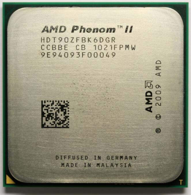
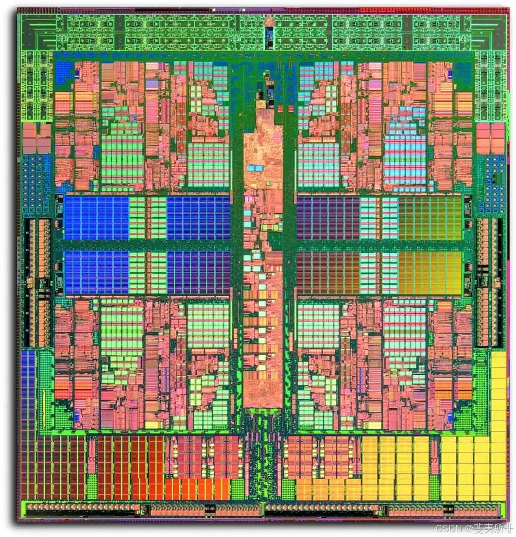
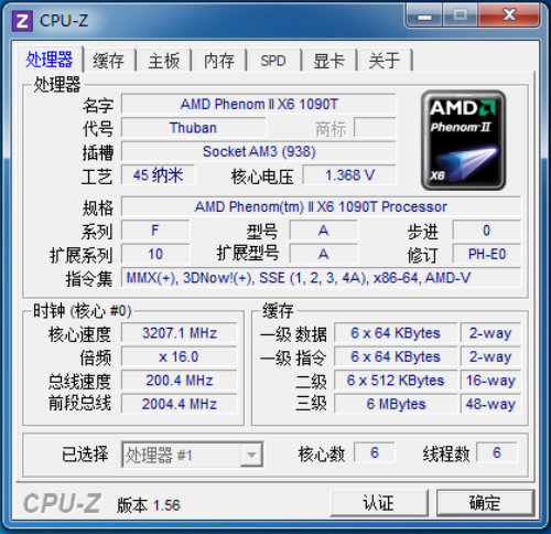
我们把时间倒退到 2010 年,当时的 AMD 在旗舰处理器上并不是 Intel 的对手。Intel 在 2010 年战意火爆,发布了当时很强大的 Intel Core i7 980X Extreme 处理器,这也是世界上第一款桌面级 6 核心处理器,AMD 当时的对策不多,但还是发布了自己的 6 核心处理器 - 羿龙 AMD Phenom II X6 1090T 作为回应,其架构依然沿用 AMD K10,可以看作是 Phenom II X4 增加两个核心而来,采用 45nm 工艺制造,核心代号为 Thuban。
这款处理器在工艺上落后于 Intel 的最新工艺 32nm,并且 Intel Core i7 980X Extreme 是支持超线程技术的,6 核心 12 线程。而 AMD Phenom II X6 1090T 只有 6 核心 6 线程。综合多种原因,那一年风光无两的处理器自然不是这款 AMD Phenom II X6 1090T,并且在接下来的一段时间内,Intel 一直保持了自己的优势地位,市场占有率高的吓人,Intel 当年的强大让 AMD 难以望其项背。
2011 年:“推土机” FX-8130P 处理器来袭但性能让人不满意
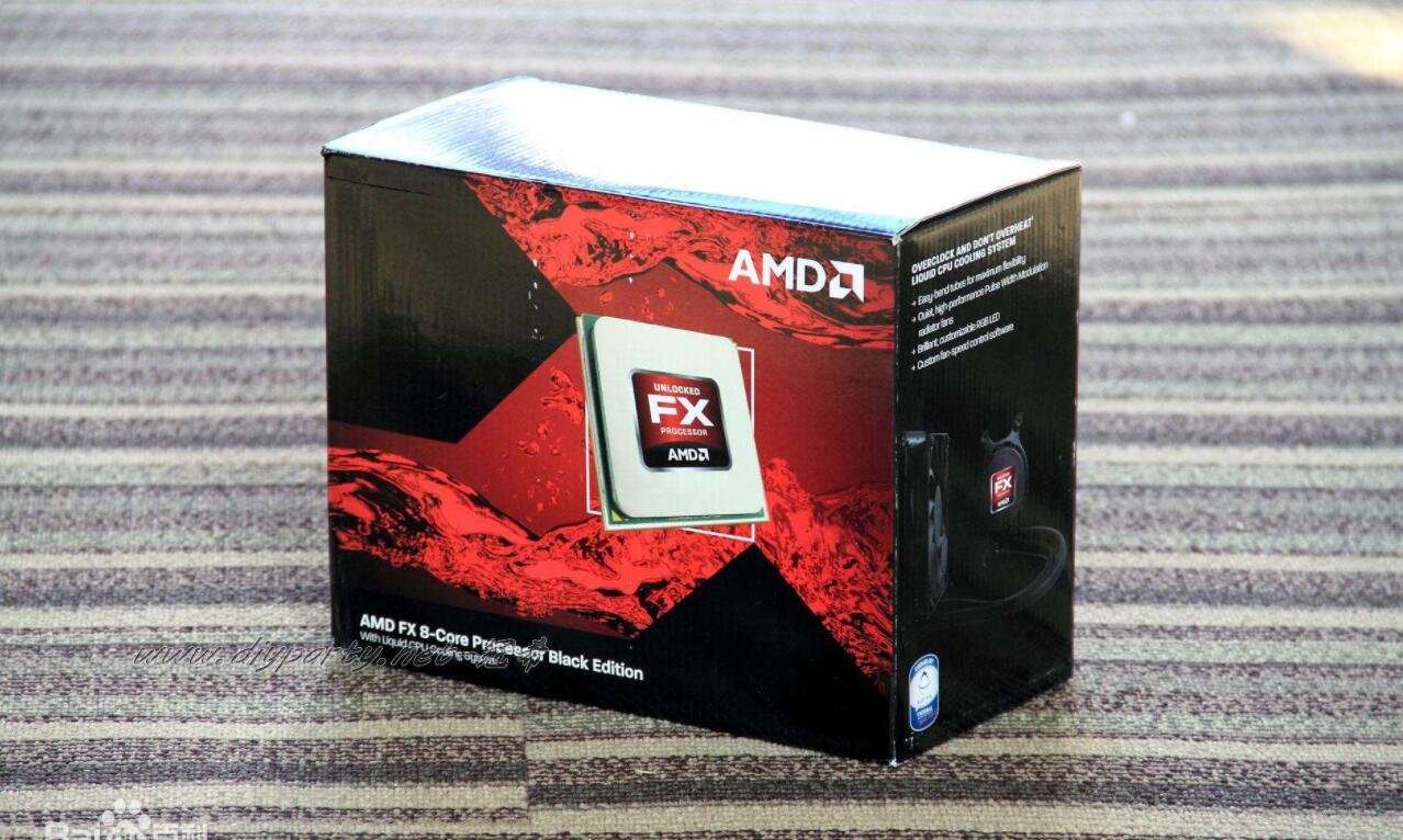
在看到竞争对手的 “酷睿系列” 处理器如此强大的性能之后,AMD 决定也研发新的 CPU 架构,对 Intel 展开绝地反击。因此在 2011 年 10 月,AMD 推出了重整旗鼓之后的作品,采用 “Bulldozer” 架构的 AMD FX 处理器。而 AMD 也在此次的 “Bulldozer” 核心中使用了大量新技术,堪称 AMD K8 之后最大的革新,他改变多了传统的 CPU 设计思路,将 CPU 模块化,而每个模块有课细分为两个为内核,这两个微内核既相互独立有高度共享浮点单元。
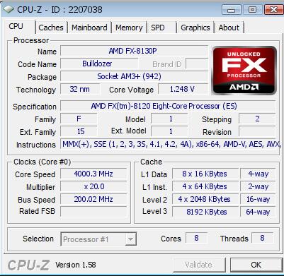
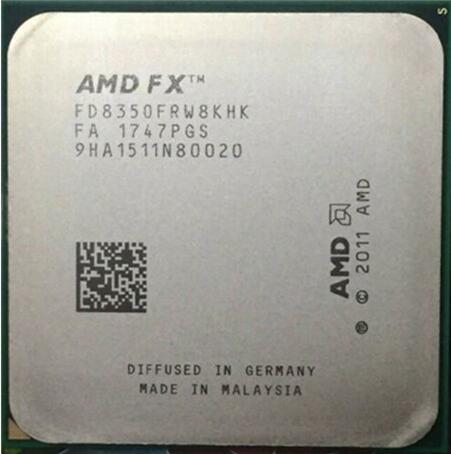
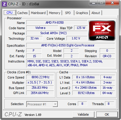
其中最为强大的处理器当属这个 FX-8130P 了,这次 AMD 终于用上了 32nm 工艺,只不过是对外宣传的 “8 核心 8 线程” 却成为了 AMD 不想回顾的记忆。因为推土机架构的缘故,每一个 CPU 的小内核并没有自己独立的浮点单元,称不上满血版的核心,所以当年关于 AMD FX 系列处理器是否是 “真 8 核” 很多玩家与 AMD 之间出现争议,一些玩家甚至认为 AMD 涉嫌非法宣传,将 AMD 告上了法庭,这些都是推土机时代 AMD 的辛酸历史。性能方面也没能达到预期,单核性能羸弱,虽然超频潜力还不错,不过这并不是 Intel 处理器的对手,高频低能的帽子也是在这个时候被用户给 AMD 扣上了。
2012 年:继承者 “打桩机” FX-8350 处理器游戏性能依旧十分羸弱
AMD 当时虽然也明白自己现在的 “推土机” 架构并不能形成优势,但短时间内大改架构推掉重来也是不可能的,只能顶着头皮继续研发下去。于是基于 “打桩机” 的 AMD FX-8350 处理器就是 AMD 在 2012 年给出的答卷,虽然在多核心能力上 AMD FX-8350 还能勉强谈笑风生,但在单核心性能上已经是被 Intel 处理器甩的连车尾灯都看不见,以至于 Intel 在单线程测试以及实际游戏的表现上彻底碾压 AMD。当时的 Intel 这边只需要一颗 Intel Core i3-3220 处理器,玩游戏帧数就比你 AMD FX-8350 高,更别提更高规格的处理器了,最后闹出了 “i3 默秒全的笑话”。
2013 年:转变策略,AMD 大力发展 APU 发布 A10-6800K 处理器
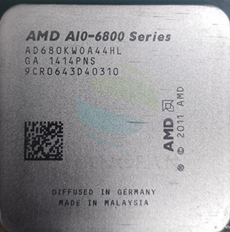
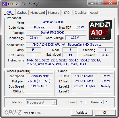
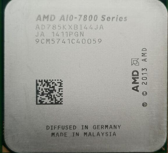
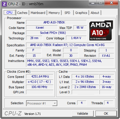
2013 年 AMD 并没有发布什么重磅级产品,唯一能拿的出手的是主流市场的 APU 产品 - AMD A10-6800K,这款产品依旧使用 32nm 工艺制作,好在内置的显卡性能还算可以,对当时注重性价比的玩家有一定吸引力,但是如果你是一个拥有独立显卡的用户,那还是 “i3 默秒全”。
2014 年:田忌赛马 A10-7850K 处理器继续打价格战
在 2014 年 AMD 决定继续使用田忌赛马的策略,既然高端市场干不过 Intel,我就把 FX 系列处理器卖的便宜一些,亲民一些,同时继续大力发展 APU,争取更多的不用独显的用户。AMD A10-7850K 就是 2014 年 AMD 的一个 APU 力作,这款处理器还是比较成功的,采用了 28nm 工艺,其内置的 GCN 架构核显 性能远超 Intel 的核显,确实为 AMD 带来了不少喜欢性价比的用户,但在整个处理器市场来看,当时的 AMD 仍然无法发布一个足以跟 Intel 抗衡的处理器。其实那个时候 “ZEN” 架构已经偷偷研发了有一段时间了,AMD 现在还需要这些老架构处理器撑一撑门面。
2015 年:AMD 无心恋战 继续发布 A10-7870K 处理器勉强撑门面
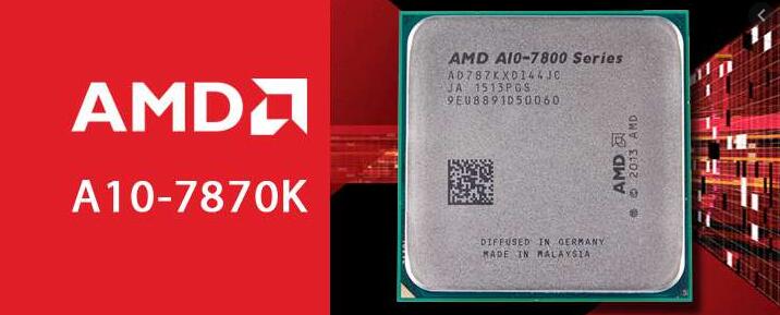
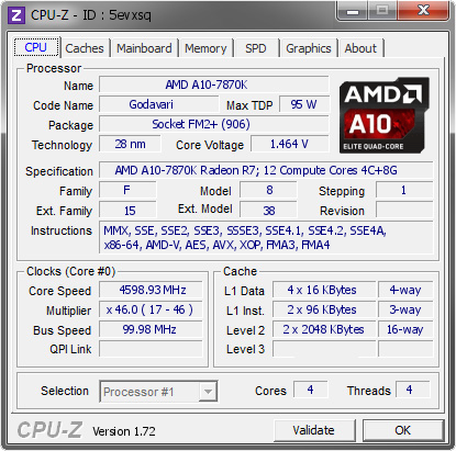
2015 年,AMD 正在对全新的 “ZEN” 架构处理器进行研发,他们在 2015 年无心恋战,只是简单的给老的 A10-7850K 升个级,提升点频率就变成了上面这个 AMD A10-7870K,由于性能真的是跟竞争对手没法相提并论,AMD 让 A10-7870K 与老 A10-7850K 价格相同,以此取代后者。
2016 年:AMD 黎明前最后的黑暗 发布 APU 小升级版本 A10-7890K 处理器
在 2016 年,AMD 终于快熬出头了,我还记得当年 2016 年 1 月 1 日元旦,我当时对着手里的乐视超级手机 1 发呆,快上大学了买一个什么电脑好呢,还是先去了解一下吧,当时我一打开 “显卡吧” 就看见满屏幕的 Intel Core i7-6700K+GTX 970 组装帖子,这一幕这么多年过去了我还是记忆犹新。可见当时玩家们根本就不关注 AMD 了,无论是显卡还是 CPU 市场,AMD 的产品都处于劣势,甚至有 “卡吧三幻” 的梗在玩家们口中流传。
但 AMD 自己并没有放弃自己,而是继续 “韬光养晦” 并 “卧薪尝胆”,AMD 继续更新了自家的 APU 系列,AMD A10-7890K 是上一年 AMD A10-7870K 升级款,在频率上有 0.2GHz 的微小提升。不过这一年为了向股东和外界证明 AMD 还有大招,时任 AMD CEO 的 Lisa Su 选择在 6 月份主动公布 “ZEN” 架构处理器的一些细节,性能提升非常大,并且明年就可以买到,这个消息让不少死忠 A 粉感到兴奋,也为整个竞争力严重不足的 CPU 市场投下了一块重磅炸弹。所以说 2016 年是 AMD 黎明前最后的黑暗年,一点也不为过。
2017 年:凤凰涅槃 “ZEN” 架构处理器横空出世 单核性能大幅提升 8 核心处理器走入百姓家
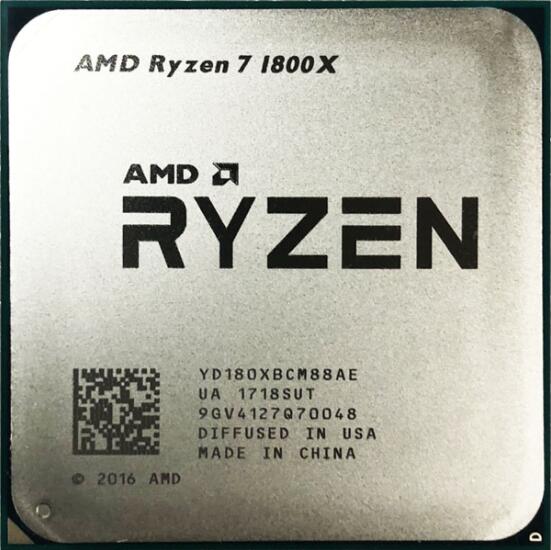
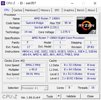
2017 年 AMD 正式发布了基于 “ZEN” 架构的第一代锐龙处理器,采用格罗方德 14nm 工艺,当时首发的旗舰型号正是上面的 AMD Ryzen 7 1800X,ZEN 架构在 IPC 性能上相比 “打桩机” 暴增 40%,全新的处理依旧采用模块化设计,不过更加主流,最小的 CPU Complex 模块(CCX)内有四个 x86 核心,每个核心都有独立的 L1 和 L2 缓存,单个模块共享 8MB L3 缓存,核心一改前代的 CMT 多线程技术,采用了更加主流的 SMT 多线程。而第一代 Ryzen 处理器采用了双 CCX 模块设计,每个 CCX 模块通过 AMD 全新设计的 Infinity Fabric 总结 / 接口连接,单个处理器就由 8 核心了,2017 年也是 “ZEN” 架构传奇之旅的元年。
从这个时候开始 Intel 才意识到情况不对,Intel Core i7-7700K 与 Intel Core i7-6700K 相比仅仅提升了一丁点频率,DIY 玩家们对此非常不爽。看到锐龙开始堆核,Intel 立即修改了自己的发展路线,也要为自己的产品线 “加核心” 了,新一轮 I/A “核战” 即将来袭。
2018 年:AMD 稳扎稳打发布 “ZEN+” 架构处理器 查缺补漏解决问题
~
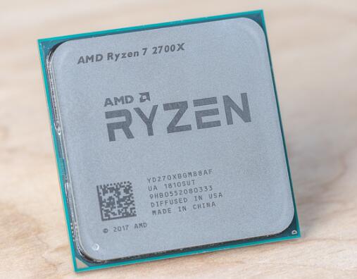
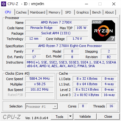
在 2018 年,AMD 再接再厉,发布 “ZEN+” 架构处理器,生产工艺是格罗方德的 12nm,略有进步。“ZEN+” 解决了不少 “ZEN” 的使用问题,比如内存兼容性等。他们推出了 AMD Ryzen 7 2700X 这颗强大的处理器,在桌面级的多核性能上领先 Intel 很多,单核性能也在逐步缩小差距。
并且自家 HEDT 平台的线程撕裂者也在有序的更新,整个 AMD CPU 部门处于良好的发展态势。此外,第一代锐龙发布会上 AMD 承诺 AM4 接口可以用到 2020 年,“ZEN+” 架构处理器的发布没有食言,老的 X370 用户依旧可以正常使用,这让当时饱受 Intel 一代一换主板的用户直呼良心,AMD 在这个时候逐渐的在 DIY 市场恢复自己的用户。
2019 年:大力反击 “ZEN2” 全面提升 发布 Ryzen 9 3950X 桌面级 16 核处理器跨平台打击对手
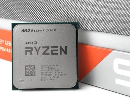
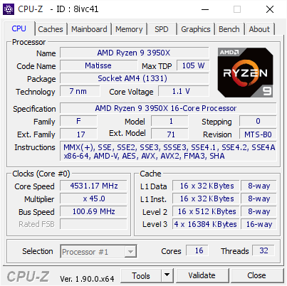
2019 年是 AMD 全力大反击的一年,“ZEN2” 架构如期而至,首先在工艺上 AMD 抛弃了 “女朋友”,选择了 TSMC 的 7nm。IPC 相比 “ZEN+” 增加 15%,提升了单核能力,还原生支持 PCIe4.0,为之后的显卡处理器共同发展打下基础。
此外之前总被大家吐槽的内存频率、延迟问题等也都有进行针对性的优化。内存频率通过 I/O 分离解决,延迟通过大容量 L3 缓存解决,这些优化最终的结果就是 AMD 在单核性能上紧紧咬住 Intel,缩小差距,在多核能力上大幅领先对手,并且桌面级旗舰处理器 AMD Ryzen 9 3950X 甚至拥有 “跨平台” 打击对手的能力,其拥有 16 个核心 32 个线程,这在之前的桌面级处理器中是不可想象的,但是 AMD 做到了。Intel 当年被粉丝们认为拥有 “10 年领先的技术储备”,现在看应该是没这么多年(笑)。(这个跟当年弗格森谈到的 “我在的时候曼城别想超过曼联是一个道理,只不过颜色互换。”)
2020 年 “ZEN3” 全方位围剿竞品 在游戏、生产力等方向继续提升
~
到了 2020 年,AM4 的承诺之期的最后一年,AMD 如约发布了 “ZEN3” 架构处理器,新的处理器性能更加 “残暴”,IPC 更是激增 “19%”!L3 直连缓存直接合并,进一步提升游戏性能,所以在之前一直没法取得优势的游戏环节,AMD 完全不虚,直接在发布会与友商旗舰处理器硬碰硬并取得优势,而多核性能 AMD 甚至在发布会上根本就没跑,答案不言自明。关于 Ryzen 5000 系列处理器的具体评测,就让我们一起期待今晚的解禁时刻吧!
尾巴
CPU 迷你天梯榜 (完整 CPU 天梯榜)
~
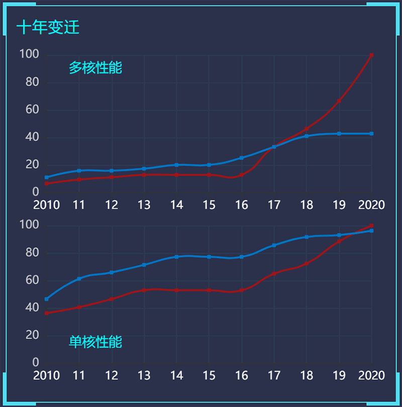
纵观 AMD 从 2010 年到 2020 年的历史,AMD 处理器的性能发生了天翻地覆的变化,从当年被寄予厚望的 “推土机” 架构遭遇滑铁卢,到现在的 “ZEN” 架构的涅槃重生,从当年被卡吧吧友调侃的 “卡巴三幻” 到现在的 “卡吧三幻” 全部实现。这中间的艰辛只有 AMD CPU 研发部门自己知道,模块化的设计思路是对的,只不过 AMD 当时的推土机处理器没有重视小核心,过分的看好显卡的发展,想让浮点运算都交给显卡去做,这些失败的经验都为 ZEN 架构的研发提供了经验教训,少走了很多弯路。有一句话说的好,AMD 锐龙的成功只不过是他 5 年前就应该做到的。好在市场需要竞争,一家独大终究不是消费者喜欢看到的,Intel 在受到 AMD 如此大的威胁之后定然不会坐以待毙,两家科技公司的共同努力才能让整个 CPU 高速进步。
此外,显卡部门也是紧随其后,在历经各种 “GCN” 魔改的显卡之后,“RDNA” 架构终于也算是在 2020 年开花结果,让 AMD 在两个领域均取得了出彩的成绩。
我本人更是亲眼见证了 AMD “ZEN” 架构的崛起全过程,我从 2016 年上大学正好也是 2020 年毕业,现在的 AM4 接口在 2020 年我认为可以称得上是圆满毕业了,那么在下一代接口上,AMD 还会带来那些惊喜呢?这真是一个让人期待的过程。
……
-
超能课堂 (249):AMD CPU 这十年,从推土机到锐龙崛起 - 超能网 杜维 发布于 2020-11-5 18:15
-
超能课堂(48):AMD显卡的红色帝国之路 - 超能网 凯恩猪蹄子发布于 2016-7-7 19:13


 1万+
1万+

 被折叠的 条评论
为什么被折叠?
被折叠的 条评论
为什么被折叠?
 到【灌水乐园】发言


