


module top(
	input clk,
	input rst_n,
	output clk_out
    );

	wire pll_clk_out;
	pll
	(
		.CLK_IN1(clk),
		.CLK_OUT1(pll_clk_out),
		.RESET(~rst_n),
		.LOCKED()
	);

	ODDR2 #(
		.DDR_ALIGNMENT("NONE"), // Sets output alignment to "NONE", "C0" or "C1"
		.INIT(1'b0),    // Sets initial state of the Q output to 1'b0 or 1'b1
		.SRTYPE("SYNC") // Specifies "SYNC" or "ASYNC" set/reset
	) ODDR2_inst (
		.Q(clk_out),   // 1-bit DDR output data
		.C0(pll_clk_out),   // 1-bit clock input
		.C1(~pll_clk_out),   // 1-bit clock input
		.CE(1'b1), // 1-bit clock enable input
		.D0(1'b1), // 1-bit data input (associated with C0)
		.D1(1'b0), // 1-bit data input (associated with C1)
		.R(1'b0),   // 1-bit reset input
		.S(1'b0)    // 1-bit set input
	);


endmodule
1、pll的复位引脚高电平有效。
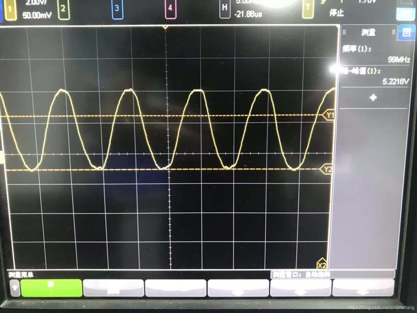
2、100mhz SMA_CLK引脚(U10 IO_L30P_GCLK1_D13_2)输出波形
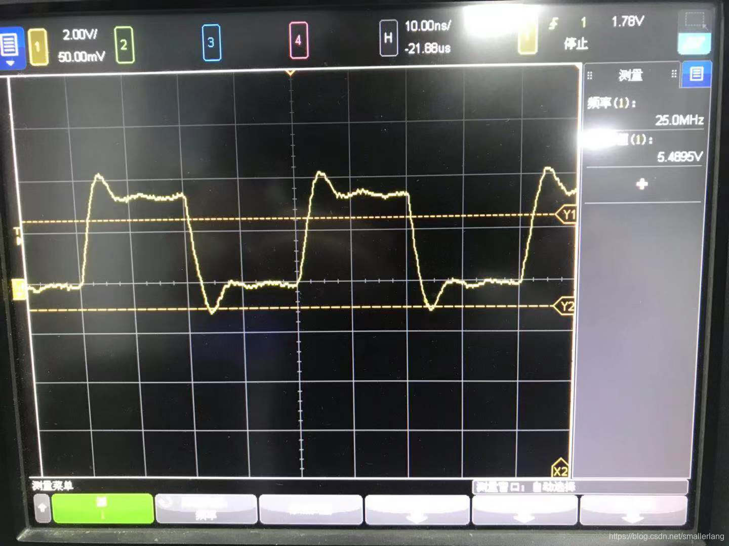
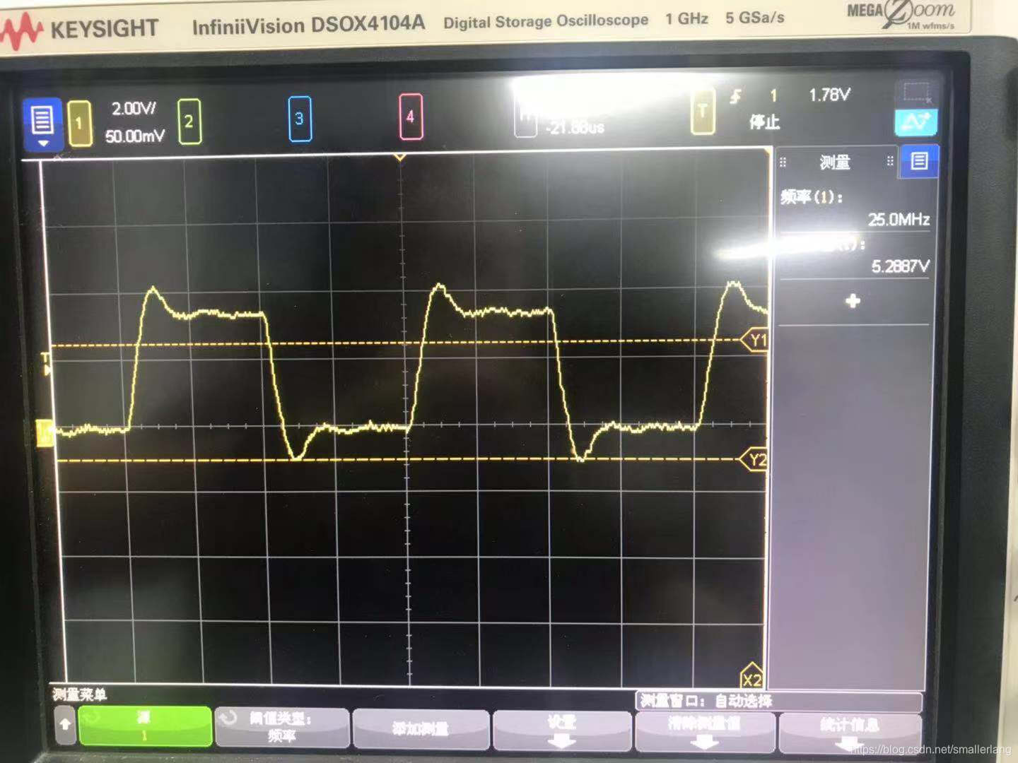
3、25mhz SMA_CLK引脚(U10 IO_L30P_GCLK1_D13_2)输出波形
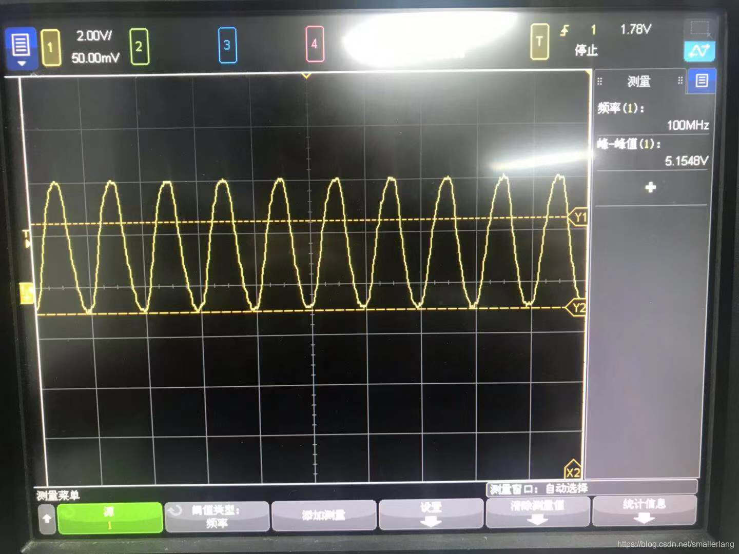
4、25mhz 普通IO引脚(N11 IO_L15N_2)输出波形
module top(
	input clk,
	input rst_n,
	output clk_out
    );

	wire pll_clk_out;
	pll
	(
		.CLK_IN1(clk),
		.CLK_OUT1(pll_clk_out),
		.RESET(~rst_n),
		.LOCKED()
	);

	reg clk_out_r;
	always @(posedge pll_clk_out or negedge rst_n)
	begin
		if(!rst_n) clk_out_r <= 1'd0;
		else clk_out_r <= ~clk_out_r;
	end

	assign clk_out = clk_out_r;


endmodule
1、100mhz SMA_CLK引脚(U10 IO_L30P_GCLK1_D13_2)直接逻辑输出波形
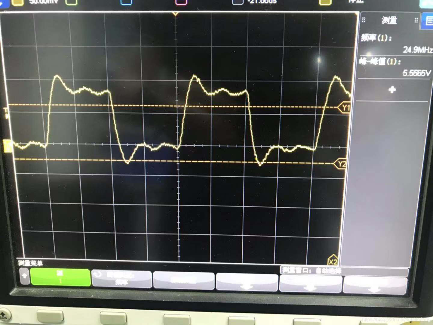
1、25mhz SMA_CLK引脚(U10 IO_L30P_GCLK1_D13_2)直接逻辑输出波形


 5762
5762


 到【灌水乐园】发言


