


 本文详细介绍Xilinx时钟约束的创建语法,包括create_clock-period、waveform选项,以及如何在Vivado中使用。还提供了高速AD转换芯片时序对齐和约束实例,强调了实际工程中对物理时钟、虚拟时钟和生成时钟的精确约束重要性。
一、Xilinx 时钟约束XDC语法
鉴于网上对时钟的介绍不全面、需要各种搜集的问题,自己整理了一篇Xilinx时钟约束进行记录。
首先,时钟约束语法如下:
create_clock -period <arg> [-name <arg>] [-waveform <args>] [-add] [-quiet] [-verbose] [<objects>]
对语法的详细讨论放在第二节中。
通过上述语法可以创建时钟约束,主要操作是约束已有物理时钟、
值得注意的是,这里的约束只是针对编译器而言的,相当于你告诉它我的时钟是什么样子的,你给我考虑它应该进行的优化。如果没有对时钟进行约束,默认按照1GHz频率进行约束,则大多数情况下会时序报错。
所以,对于工程中所有的时钟,物理时钟、生成时钟、虚拟时钟、跨时钟域等都应该详尽地告诉编译器(来自某大佬)。
二、vivado中creat_clock详解
通过在vivado Tcl Console键入命令 create_clock -help 可以得到一个官方的creat_clock帮助内容,如下:
create_clock

Description:
Create a clock object

Syntax:
create_clock  -period <arg> [-name <arg>] [-waveform <args>] [-add] [-quiet]
              [-verbose] [<objects>]

Returns:
new clock object

Usage:
  Name         Description
  ------------------------
  -period      Clock period: Value > 0
  [-name]      Clock name
  [-waveform]  Clock edge specification
  [-add]       Add to the existing clock in source_objects
  [-quiet]     Ignore command errors
  [-verbose]   Suspend message limits during command execution
  [<objects>]  List of clock source ports, pins or nets

Categories:
SDC, XDC

Description:

  Note: The XDC > Timing Constraints language templates and the Timing
  Constraints Wizard in the Vivado IDE offer timing diagrams and additional
  details around defining specific timing constraints. You can refer to these
  sources for additional information.

  Create a clock object with the specified period or waveform defined in
  nanoseconds (ns). This command defines primary clocks which are used by the
  timing engine as the delay propagation starting point of any clock edge.
  The defined clock can be added to the definition of an existing clock, or
  overwrite the existing clock.

  A virtual clock can be created that has no source in the design. A virtual
  clock can be used as a time reference for setting input and output delays
  but does not physically exist in the design.

  A clock can also be generated from an existing physical clock, and derive
  many of its properties from the master clock. Use the
  create_generated_clock command to derive a clock from an existing physical
  clock.

  Note: If you use create_clock to create a generated clock, instead of
  create_generated_clock, the created clock does not inherit any of the
  properties of its source clock. The insertion delay and jitter of the
  parent clock will not be propagated to the generated clock, causing
  incorrect timing calculations.

  The create_clock command returns the name of the clock object that is
  created.

Arguments:

  -period <arg> - (Required) Specifies the clock period of the clock object
  to be created. The value is specified as nanoseconds (ns) and must be
  greater than zero (>0).

  -name <arg> - (Optional) The name of the clock object to be created. If the
  name is omitted, a system-generated name will be used based on the
  specified source <objects>. You can also use the -name option without
  source <objects> to create a virtual clock for the design that is not
  associated with a physical source on the design.

  -waveform <arg1 arg2 ...> - (Optional) The rising and falling edge times of
  the waveform of the defined clock, in nanoseconds, over one full clock
  cycle. You can use multiple rising and falling edges to define the
  characteristics of the waverform, but there must be an even number of
  edges, representing both the rising and falling edges of the waveform. The
  first time specified (arg1) represents the time of the first rising
  transition, and the second time specified (arg2) is the falling edge. If
  the value for the falling edge is smaller than the value for the rising
  edge, it means that the falling edge occurs before the rising edge.

  Note: If you do not specify the waveform, the default waveform is assumed
  to have a rising edge at time 0.0 and a falling edge at one half the
  specified period (-period/2).

  -add - (Optional) Define multiple clocks on the same source for
  simultaneous analysis with different clock waveforms. Use -name to specify
  the new clock to add. If you do not specify this option, the create_clock
  command will overwrite any existing clock of the same name.

  -quiet - (Optional) Execute the command quietly, returning no messages from
  the command. The command also returns TCL_OK regardless of any errors
  encountered during execution.

  Note: Any errors encountered on the command-line, while launching the
  command, will be returned. Only errors occurring inside the command will be
  trapped.

  -verbose - (Optional) Temporarily override any message limits and return
  all messages from this command.

  Note: Message limits can be defined with the set_msg_config command.

  <objects> - (Optional) The ports, pins, or nets which are the source of the
  specified clock. If you specify a clock on a source object that already has
  a clock, the new clock will overwrite the original clock unless you also
  specify the -add option. If no <objects> are specified to attach the clock
  object to, the clock will be created as a virtual clock in the design.

  Note: The first driver pin of a specified net will be used as the source of
  the clock.

Examples:

  The following example creates a physical clock called bftClk and defines
  the clock period:

    create_clock -name bftClk -period 5.000 [get_ports bftClk]


  Note: If the get_ports command defining the objects is left off of this
  example, a virtual clock is created in the design rather than a physical
  clock.

  The following example creates a clock named clk on the input port, bftClk,
  with a period of 10ns, the rising edge at 2.4ns and the falling edge at
  7.4ns:

    create_clock -name clk -period 10.000 -waveform {2.4 7.4} [get_ports bftClk]


  The following example creates a virtual clock since no clock source is
  specified:

    create_clock -name virtual_clock -period 5.000


  The following example creates a clock with the falling edge at 2ns and the
  rising edge at 7ns:

    create_clock -name clk -period 10.000 -waveform {7 2} [get_ports bftClk]


  Note: Because the falling edge is earlier than the rising edge in the
  -waveform definition, although it is specified as arg2, it occurs first in
  the waveform.

See Also:

   *  all_clocks
   *  create_generated_clock
   *  get_clocks
   *  report_clocks
   *  report_clock_interaction
   *  report_clock_networks
   *  report_clock_utilization
   *  set_clock_groups
   *  set_clock_latency
   *  set_clock_uncertainty
   *  set_input_delay
   *  set_output_delay
   *  set_propagated_clock
有需要的可以自己进行翻译,大致意思如下:
| Name | Description |
|---|---|
| -period | 时钟周期,值>0 |
| [-name] | 时钟名字 |
| [-waveform] | 时钟沿的规范 |
| [-add] | 添加一个钟 |
| [-quiet] | 忽略命令错误 |
| [-verbose] | 在命令执行期间暂停消息限制 |
| [< objects >] | 时钟源端口,引脚或网的列表 |
利用这个语法:
- 你可以创建一个钟,这个钟来自现有时钟,其被定义的波形信息将替代原有钟。
- 你可以创建一个虚拟钟,这个虚拟中可以作为设计的输入输出间延迟做参考,但是该钟并不存在。
- 也可以从现有的物理时钟中派生一个时钟,其参数来自于现有时钟。
- 如果使用create_clock创建一个生成的时钟,而不是create_generated_clock,所创建的时钟不继承任何源时钟属性的插入延迟和抖动,父时钟将不会传播到生成的时钟,导致不正确的时间计算。
周期的典型值是4.032ns,精度到小数点后3位,代表了248MHz输入的一个时钟。名字在指定后将替代右端object名字,并在约束文件中起作用。波形是比较重要的信息,其可以使用多个上升边和下降边来定义波形特征,但必须有偶数个边.(arg1)表示第一次上升的时间转换,并且指定的第二次时间(arg2)是下降边缘。如果下降边的值小于上升边的值边缘,它意味着下降的边缘出现在上升的边缘之前。
三、高速AD转换芯片约束实例
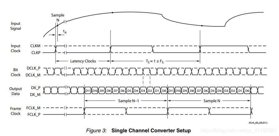
AD芯片的通用时序图如图所示,利用bit clock的双沿进行bit接收。在高速AD经过LVDS口接入FPGA时,由于综合和走线的原因,bit clock进入PLL再回到logic中与frame和bit对应时,其相位关系会发生改变。此时需要对bit clock进行相位对齐。
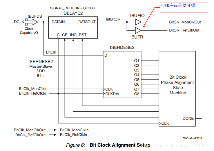
如图所示为相位对齐的结构图,bit clock即DCLK,经过IDELAY2进行延迟,然后再ISERDESE2串转并对bit clock检测。通过检测结果动态调节DCLK找到时钟上升沿进行对齐,然后相位关系就调整回进入FPGA时的状态了。
下方则对上述时钟时序进行约束。
约束一般时钟输入引脚,这里将PCB板上输入给FPGA的时钟进行约束
按照第二节所讲,create一个有时钟源的时钟,会将原时钟覆盖,除非使用add命令。
create_clock -period 16.129 [get_ports FPGA_CLK_P]
约束ADbit同步引脚并重命名
将引脚重命名为AdcBitClk,上升沿从0ns开始,下降沿在2.016ns处,即占空比50%,移相0度。
create_clock -period 4.032 -name AdcBitClk -waveform {0.000 2.016} [get_ports DCLK_p_pin]
去掉这条路径上的时序检查,因为这条路径时钟是我自己用idelay调节的,所以时序检查对这没有用,反而会报一些critical warnning。这仅适用于忽略时序检查的地方。
set_false_path -from [get_ports AD_DCO_P] -through [get_cells AD/ADC_Top/AdcToplevel_Toplevel_I_AdcToplevel/AdcToplevel_I_AdcClock/AdcClock_I_Isrds_Master] -through [get_cells AD/ADC_Top/AdcToplevel_Toplevel_I_AdcToplevel/AdcToplevel_I_AdcClock/AdcClock_I_Bufio] -to [get_cells -hierarchical *Isrds*]
创建一个生成时钟。
create_generated_clock -name AdcBitClkDiv -source [get_pins AD/ADC_Top/AdcToplevel_Toplevel_I_AdcToplevel/AdcToplevel_I_AdcClock/AdcClock_I_Isrds_Master/DDLY] -divide_by 4 [get_nets -hierarchical *IntClkDiv*]
这个实例是我在项目中实际用到的,本人对时钟约束可能存在一些理解上的不足,欢迎大家指正。


 1万+
1万+

 被折叠的 条评论
为什么被折叠?
被折叠的 条评论
为什么被折叠?
 到【灌水乐园】发言


