


写在前面
本系列文章主要讲解德州仪器(TI)TDA4VM芯片的相关知识,希望能帮助更多的同学认识和了解德州仪器(TI)TDA4VM芯片。
若有相关问题,欢迎评论沟通,共同进步。(*^▽^*)
错过其他章节的同学可以电梯直达目录↓↓↓
TDA4VM芯片
6. 时序和开关特性
6.2 电源时序
6.2.4 隔离MCU域和主域的上电时序
隔离MCU域和主电压域使SoC的MCU和主处理器子系统能够独立运行。SoC的PDN设计可能需要支持独立的MCU和主处理器功能有2个原因。第一个是为了提供灵活性,使SoC能够进入低功耗模式,当不需要处理器操作时,可以显著降低SoC的功耗。第二个是为了实现稳定性,避免单个故障同时影响MCU和主处理器子系统,这在使用SoC的MCU作为系统安全监控处理器时特别有益。所需的额外PDN电源导轨数量取决于不同MCU IO信号电压等级的数量。如果只使用1.8V IO信号,则仅需要2个额外的电源轨。如果需要1.8V和3.3V的输入输出信号,则需要4个额外的电源轨。图6描述了隔离MCU域和主域的上电时序。
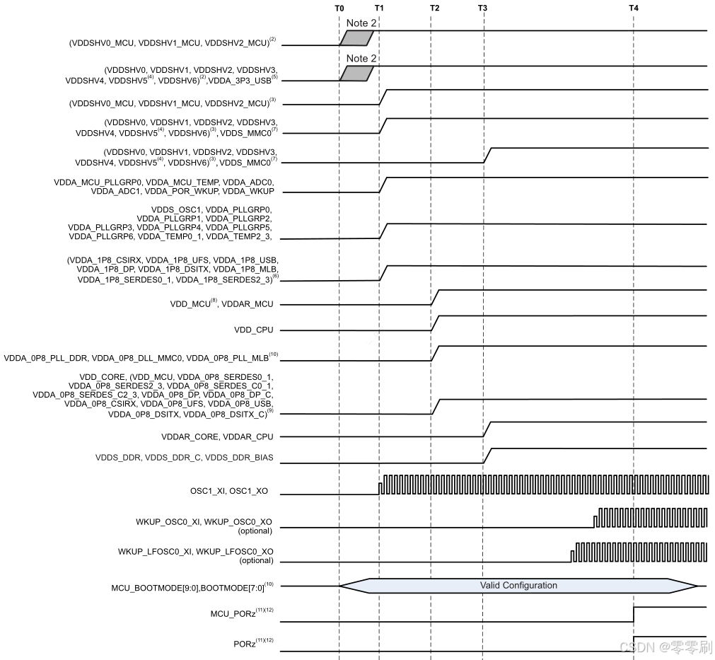
图 6 隔离MCU域和主域的上电时序
1. 时间戳标记
T0 – 3.3V voltages start ramp-up to V OPR MIN . (0ms)
T1 – 1.8V voltages startramp-up to V OPR MIN . (2ms)
T2 – Low voltage core supplies start ramp-up to V OPR MIN . (3ms)
T3 – Low voltage RAM array voltages start ramp-up to V OPR MIN . (4ms)
T4 – OSC1 is stable and PORz/MCU_PORz are de-asserted to release processor from reset. (13ms)
2. Any MCU or Main dual voltage IO supplies (VDDSHVn_MCU or VDDSHVn) being supplied by 3.3V tosupport 3.3V digital interfaces. A few supplies could have varying start times between T0 to T1 due to PDN designs using different power resources with varying turn-on & ramp-up time delays.
3. Any MCU or Main dual voltage IO supplies (VDDSHVn_MCU or VDDSHVn) being supplied by 1.8V tosupport 1.8V digital interfaces. When eMMC memories are used, Main 1.8V supplies could have delayed start times that aligns to T3 due to PDN designs grouping supplies with VDD_MMC0.
4. VDDSHV5 supports MMC1 signaling for SD memory cards. If compliant UHS-I SD card operation is needed,then an independent, dual voltage (3.3V/1.8V) power source and rail are required. The start of ramp-up to 3.3V will be same as other 3.3V domains as shown. If SD card is not needed or standard data rates with fixed 3.3V operation is acceptable, then supply can be grouped with digital IO 3.3V power rail. If a SD card is capable of operating with fixed 1.8V, then supply can be grouped with digital IO 1.8V power rail.
5. VDDA_3P3_USB is 3.3V analog supply used for USB 2.0 differential interface signaling. A low noise, analogsupply is recommended to provide best signal integrity for USB data eye mask compliance. The start of ramp-up to 3.3V will be same as other 3.3V domains as shown. If USB interface is not needed or data bit errors can be tolerated, then supply can be grouped with 3.3V digital IO power rail either directly or through a supply filter.
6. VDDA_1P8_<phy> are 1.8V analog supplies supporting multiple serial PHY interfaces. A low noise, analogsupply is recommended to provide best signal integrity, interface performance and spec compliance. If any of these interfaces are not needed, data bit errors or non-compliant operation can be tolerated, then supplies can be grouped with digital IO 1.8V power rail either directly or through an in-line supply filter is allowed.
7. VDD_MMC0 is 1.8V digital supply supporting MMC0 signaling for eMMC interface and must ramp up at timestamp T3. Any MCU or Main dual voltage IO operating at 1.8V can be grouped with VDD_MMC0 into a common power rail with a ramp-up at time stamp T3. If MMC0 or eMMC0 interface is not needed, then domain can be grouped with digital IO 1.8V power rail with ramp-up at time stamp T1.
8. VDD_MCU is a digital voltage supply with a wide operational voltage range and power sequencing flexibility,enabling it to be grouped and ramped-up with either 0.8V VDD_CORE at time stamp T2 or 0.85V RAM array domains (VDDAR_xxx) at time stamp T3.
9. VDDA_1P8_<clk/pll/ana> are 1.8V analog supplies supporting clock oscillator, PLL and analog circuitryneeding a low noise supply for optimal performance. It is not recommended to combine analog VDDA_1P8_<phy> domains or digital VDDSHVn_MCU and VDDSHVn IO domains since high frequency switching noise could negatively impact jitter performance of clock, PLL and DLL signals.
10. VDDA_0P8_<dll/pll> are 0.8V analog supplies supporting PLL and DLL circuitry needing a low noise supplyfor optimal performance. It is not recommended to combine these domains with any other 0.8V domains since high frequency switching noise could negatively impact jitter performance of PLL and DLL signals.
11. Minimum set-up and hold times shown with respect to MCU_PORz and PORz asserting high to latchMCU_BOOTMODEn (referenced to MCU_VDDSHV0) and BOOTMODEn (reference to VDDSHV2) settings into registers during power up sequence.
12. Minimum elapsed time from crystal oscillator circuitry being energized (VDDS_OSC1 at T1) until stable clock frequency is reached depends upon on crystal oscillator, capacitor parameters and PCB parasitic values. A conservative 10ms elapsed time defined by (T4 – T1) time stamps is shown. This could be reduced depending upon customer’s clock circuit (that is, crystal oscillator or clock generator) and PCB designs.
本文章是博主花费大量的时间精力进行梳理和总结而成,希望能帮助更多的小伙伴~ 🙏🙏🙏
后续内容将持续更新,敬请期待(*^▽^*)
欢迎大家评论,点赞,收藏→→→


 2057
2057

 被折叠的 条评论
为什么被折叠?
被折叠的 条评论
为什么被折叠?
 到【灌水乐园】发言


