德州仪器(TI)—TDA4VM芯片详解(4)—时序和开关特性

写在前面

本系列文章主要讲解德州仪器(TI)TDA4VM芯片的相关知识,希望能帮助更多的同学认识和了解德州仪器(TI)TDA4VM芯片。

若有相关问题,欢迎评论沟通,共同进步。(*^▽^*)


错过其他章节的同学可以电梯直达目录↓↓↓

德州仪器(TI)—TDA4VM芯片详解—目录-优快云博客


TDA4VM芯片

5. PIN定义

如图2示意了FCBGA-N827封装的PIN脚定义。

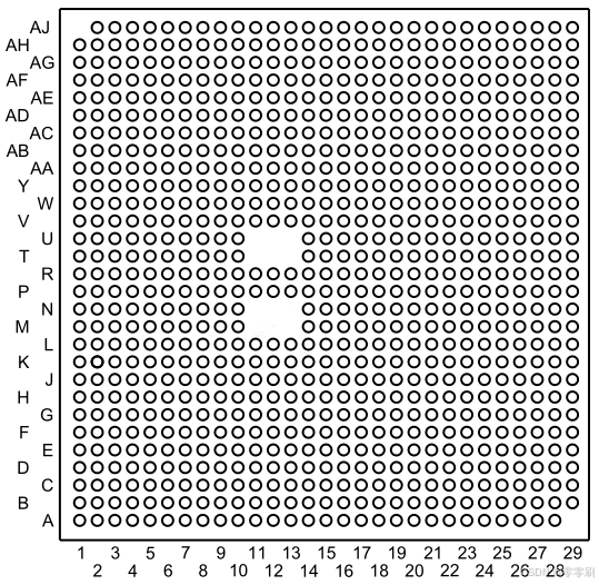
图 2 FCBGA-N827封装PIN脚定义(底部视角)

6. 时序和开关特性

6.1  时序参数和信息

表2是时间参数下标说明,如表所示。

缩写

参数

c

Cycle time (period)

d

Delay time

dis

Disable time

en

Enable time

h

Hold time

su

Setup time

START

Start bit

t

Transition time

v

Valid time

w

Pulse duration (width)

X

Unknown, changing, or don't care level

F

Fall time

H

High

L

Low

R

Rise time

V

Valid

IV

Invalid

AE

Active Edge

FE

First Edge

LE

Last Edge

Z

High impedance

表 2 时间参数下标说明

6.2 电源时序

本节描述了为确保设备正常运行所需的电源时序。设备可以使用隔离或组合MCU域和主域电源分配网络(PDN)进行操作。基于隔离和组合MCU域和主域PDN,建议使用两种不同的主电源时序。此外,设备可以在MCU域或DDR保留低功耗模式下操作。显示了两种不同的低功耗模式进入和退出所需的设备电源时序。

 6.2.1 电源切换率需求

为了保持内部静电防护装置的安全工作范围,TI建议将电源的最大切换速率限制在100 mV/us以下,如图3所示。例如,1.8V电源的斜坡时间应大于18us,以确保转换率小于100 mV/us。

图 3 电源切换和切换率

 6.2.2 组合MCU域和主域的上电时序

图4描述了当类似的MCU域和主域组合到公共电源轨时,主要的上电顺序。结合MCU域和主域,通过减少电源轨和电源的总数,同时使MCU域和主域子系统依赖公共电源轨运行,简化了PDN设计。

图 4 组合MCU域和主域的上电时序

 1. 时间戳标记  

T0 – 3.3V voltages start ramp-up to V OPR MIN. (0ms)

T1 – 1.8V voltages start ramp-up to V OPR MIN. (2ms)

T2 – Low voltage core supplies start ramp-up to V OPR MIN. (3ms)

T3 – Low voltage RAM array voltages start ramp-up to V OPR MIN. (4ms)

T4 – OSC1 is stable and PORz/MCU_PORz are de-asserted to release processor from reset. (13ms)

2. Any MCU or Main dual voltage IO supplies (VDDSHVn_MCU or VDDSHVn) being supplied by 3.3V tosupport 3.3V digital interfaces. A few supplies could have varying start times between T0 to T1 due to PDN designs using different power resources with varying turn-on & ramp-up time delays.

 3. Any MCU or Main dual voltage IO supplies (VDDSHVn_MCU or VDDSHVn) being supplied by 1.8V tosupport 1.8V digital interfaces. When eMMC memories are used, Main 1.8V supplies could have a ramp-up aligned to T3 due to PDN designs grouping supplies with VDD_MMC0.

 4. VDDSHV5 supports MMC1 signaling for SD memory cards. If compliant high-speed SD card operation isneeded, then an independent, dual voltage (3.3V/1.8V) power source and rail are required. The start of ramp-up to 3.3V will be same as other 3.3V domains as shown. If SD card is not needed or standard data rates with fixed 3.3V operation is acceptable, then domain can be grouped with digital IO 3.3V power rail. If a SD card is capable of operating with fixed 1.8V, then domain can be grouped with digital IO 1.8V power rail.

 5. VDDA_3P3_USB is 3.3V analog domain used for USB 2.0 differential interface signaling. A low noise,analog supply is recommended to provide best signal integrity for USB data eye mask compliance. The start of ramp-up to 3.3V will be same as other 3.3V domains as shown. If USB interface is not needed or data bit errors can be tolerated, then domain can be grouped with 3.3V digital IO power rail either directly or through a supply filter.

 6. VDDA_1P8_<phy> are 1.8V analog domains supporting multiple serial PHY interfaces. A low noise, analogsupply is recommended to provide best signal integrity, interface performance and spec compliance. If any of these interfaces are not needed, data bit errors or non-compliant operation can be tolerated, then domains can be grouped with digital IO 1.8V power rail either directly or through an in-line supply filter is allowed.

 7. VDD_MMC0 is 1.8V digital supply supporting MMC0 signaling for eMMC interface. If MMC0 or eMMC0interface is not needed, then domain can be grouped with digital IO 1.8V power rail with power up time stamp at T1. However, if MMC0 interface is needed, then VDD_MMC0 must not start ramp-up until time stamp T3 after VDD_CORE has reached V OPR MIN . Any MCU or Main dual voltage IO operating at 1.8V can be grouped with VDD_MMC0 into a common power rail with power up time stamp T3.

 8. VDD_MCU is a digital voltage supply with a wide operational voltage range and power sequencing flexibility,enabling it to be grouped and ramped-up with either 0.8V VDD_CORE at time stamp T2 or 0.85V RAM array domains (VDDAR_xxx) at time stamp T3.

 9. VDDA_1P8_<clk/pll/ana> are 1.8V analog domains supporting clock oscillator, PLL and analog circuitryneeding a low noise supply for optimal performance. It is not recommended to combine analog VDDA_1P8_<phy> domains or digital VDDSHVn_MCU and VDDSHVn IO domains since high frequency switching noise could negatively impact jitter performance of clock, PLL and DLL signals.

 10. VDDA_0P8_<dll/pll> are 0.8V analog domains supporting PLL and DLL circuitry needing a low noise supply for optimal performance. It is not recommended to combine these domains with any other 0.8V domains since high frequency switching noise could negatively impact jitter performance of PLL and DLL signals.

 11. Minimum set-up and hold times shown with respect to MCU_PORz and PORz asserting high to latchMCU_BOOTMODEn (referenced to MCU_VDDSHV0) and BOOTMODEn (reference to VDDSHV2) settings into registers during power up sequence.

 12. Minimum elapsed time from crystal oscillator circuitry being energized (VDDS_OSC1 at T1) until stable clock frequency is reached depends upon on crystal oscillator, capacitor parameters and PCB parasitic values. A conservative 10ms elapsed time defined by (T4 – T1) time stamps is shown. This could be reduced depending upon customer’s clock circuit (that is, crystal oscillator or clock generator) and PCB designs.


本文章是博主花费大量的时间精力进行梳理和总结而成,希望能帮助更多的小伙伴~  🙏🙏🙏

后续内容将持续更新,敬请期待(*^▽^*)

欢迎大家评论,点赞,收藏→→→

评论
添加红包

请填写红包祝福语或标题

红包个数最小为10个

红包金额最低5元

当前余额3.43前往充值 >
需支付:10.00
成就一亿技术人!
领取后你会自动成为博主和红包主的粉丝 规则
hope_wisdom
发出的红包

打赏作者

零零刷

你的鼓励将是我创作的最大动力

¥1 ¥2 ¥4 ¥6 ¥10 ¥20
扫码支付:¥1
获取中
扫码支付

您的余额不足,请更换扫码支付或充值

打赏作者

实付
使用余额支付
点击重新获取
扫码支付
钱包余额 0

抵扣说明:

1.余额是钱包充值的虚拟货币,按照1:1的比例进行支付金额的抵扣。
2.余额无法直接购买下载,可以购买VIP、付费专栏及课程。

余额充值