


 本文详细介绍了FlashSpi模块作为SPI主控制器的特性,包括通过AHB总线配置,支持多种SPI从设备,灵活的通信阶段设计,以及模块的接口和功能。还讨论了系统集成方法和注意事项。
- Overview
1.1. Characteristics of this spi controller
The FlashSpi module is an spi master controller that can be configured through AHB bus. It is suitable for wifi chips based on AHB bus architecture like S902, and is used to read and write off-chip
flash chips such as S25FL116K of Spansion, W25Q20CL of Winbond or similar off-chip flash chips
that provide spi slave interface. This module has the following features:
- provide a set of AHB slave interfaces, a set of DMA Single request interfaces and an interrupt request in the chip, and provide spi master interfaces outside the chip.
- It can provide spi clock with the fastest half of the system clock frequency.
- For a communication, it starts automatically after the register is configured. After the communication is completely finished, the register flag bit is displayed, and the completion interrupt can also be generated.
- One communication can contain up to 8 independently configurable phase, which is enough to flexibly correspond to various situations contained in one spi communication of flash chip.
- The whole module adopts synchronous clock design, and all signals belong to CLK clock domain.
1.2, the concept of PHASE
The following figure is a typical timing diagram of reading FLASH data through SPI.
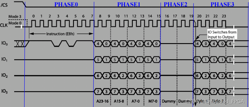
The process from CSn falling to CSn rising is called an SPI communication. In the SPI communication shown above, Instruction, A, M and Dummy should be sent in turn, and then data should be received. And Instruction only uses one line, while the subsequent processes all use four lines. Aiming at this kind of timing, this module puts forward the concept of PHASE. A communication can contain up to 8 PHASEs, and each phase can independently set parameters such as read-write
operation, 1/2/4 line mode, communication data volume, etc. After the first SPI communication starts, this module will finish the tasks set by each PHASE in the order of PHASE0→PHASE7, and then end the SPI communication. For example, for the timing of the above figure, it can be divided into 4 PHASE.
1.3. Module block diagram
The following figure is a block diagram of this spi controller:
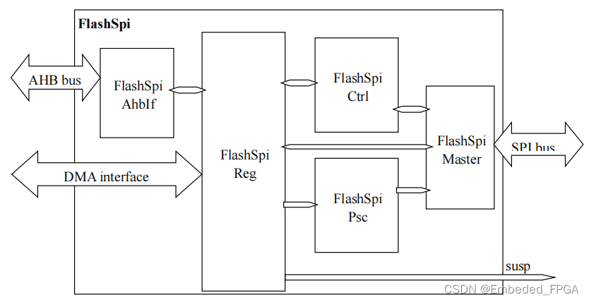
FlashSpiAhbIf: an AHB Slave interface controller, which is responsible for converting the AHB bus signal into the internal read-write signal of the module and interacting with the register module FlashSpiReg to complete the read-write operation.
Flaspireg: register module of SPI controller, in which all registers are located. At the same time, the generation and processing of DMA interface signals and the generation of interrupts are also in this module.
Flaspictrl: the core control module of SPI controller. When it is detected that the SPI_START bit in FlashSpiReg is written as 1, the phase set in the register is analyzed to generate control and data for FlashSpiDataPump.
FlashSpiPsc:spi sck clock controller, used to control the frequency of sck clock.
FlashSpimaster: Spimaster interface controller, which controls the spi bus to send and receive according to the control signal sent by FlashSpiCtrl.
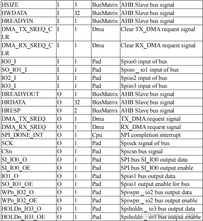
1.4. Top port
The following is a list of top-level ports and functions of this module: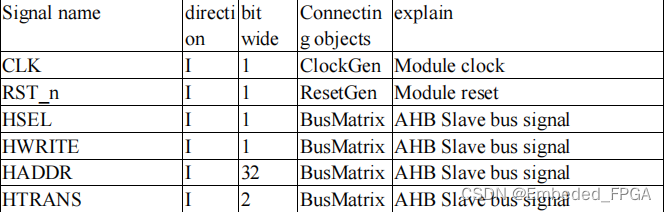
2. Instructions for use of the module
2.1. System integration method
The integration of AHB bus, DMA interface and interrupt interface is relatively simple, which will not be described here. The integration of SPI bus should be equivalent to the following logic: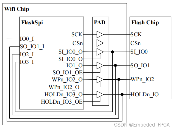
In addition, in order to prevent the input from floating, it is best to add a pull up resistor between Wifi Chip and Flash Chip.


 6984
6984

 被折叠的 条评论
为什么被折叠?
被折叠的 条评论
为什么被折叠?
 到【灌水乐园】发言


