


 本文介绍了商业FPGA的时钟网络结构,包括Altera Strataix II和Xilinx Virtex II Pro的全球和局部时钟网络。讨论了全交叉bar和集中器网络,并提出了一种参数化的时钟网络模型,该模型采用三级时钟分布拓扑。总结指出,在逻辑块、肋骨和脊中增加时钟输入的数量对面积和功率的影响不同,需要权衡。
commercial clock networks:
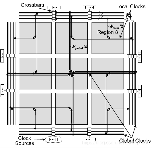
current commercial FPGA support multiple and local and global clock domains. the FPGA is divided into four quadrants.
Altera Straitix II provides 16 global clock signals, which can be connected to all the FFs on the FPGA, and 8 local clock networks in each of four quadrant, which can be connected to all the FFs within the quadrant.

Xilinx Virtex II Pro devices provide 16 global clock networks and 8 locak clock networks, unlike Altera devices, however, the global clocks in the Virtex II Pro are not connected to FFs directly, instead, the global clocks drive local clocks within each quadrant.

within a quadrant, the clocks are distributed to rows of logic blocks through a row MUX and rib routing channels.
in Stratix II devices, each row MUX chooses 6 clocks from 16+8 clocks and provides them to all FFs in that row:

in Virtex II devices, the row MUX choose between 8 local clocks.
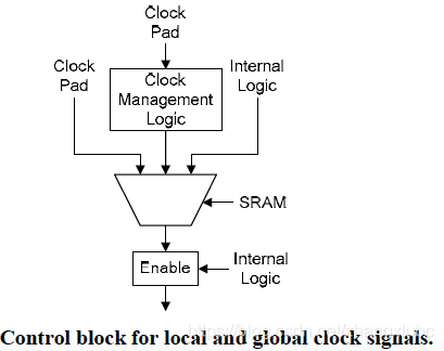
the circuits that drive the clock networks are similar between the above two, and can be driven by external source, internal source, or by clock management circuits (e.g. PLL).
full crossbar and concentrator networks
An n x m single-stage crossbar is shown below, n*m switches are required and any inputs can be connected to any outputs.
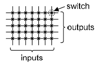
an concentrator network with m-element set of the n-input signals can be mapped to m outputs, this concentrator contains m*(n-m+1) switches. this sparse crossbar is most efficient when m is close to n (i.e. like a square).
parameterized clock network model
the networks in this model use a three-stage clock distribution topology:
- the first stage programmably connects some number of clcoks sources (clock pads, PLL/DLL outputs, or internal signals) to the center of some number of clock regions.
- the second stage programmably distributes the clocks to the logic blocks within each region.
- the third stage connects the clocks inputs of each logic block to the FFs within that logic block.
the parameters used to describe the clock networks are listed here:
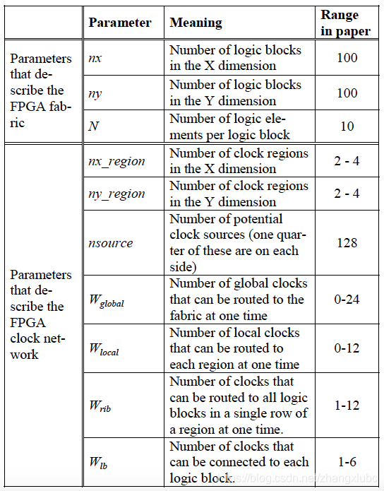
- clock sources: The clock signals will typically be driven by selected outputs from PLL/DLL, dedicated input pads, or signals from the FPGA core. In all cases, we assume the sources are distributed evenly around the periphery of the FPGA core. In our model, the number of potential clock sources is nsource, meaning there are nsource/4 potential clock sources on each side of the FPGA.
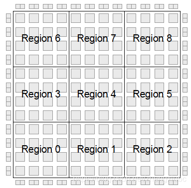
- global and local clock regions: assume global clocks are distributed across the entire chip (but not necessarily to every logic block), local clocks are distributed only in a region of FPGA. by distributing the global clocks to each region using a dedicated network, lower skew for these clocks can be achived. an 3x3 (nx_region x ny_region, and in the commercial FPGA mentioned before, it's 2 x 2)clock regions example is shown below. to support local clocks, the FPGA fabric is broken down into a number of regions, each of which can be driven by a different set of local clocks (the same local clock can also be connected to more than one region).
1st network stage:
- The first stage of the clock network programmably connects the clock sources on the periphery of the chip to the center of each region. The first stage consists of two parallel networks: one for the global clocks (Wglobal) and one for the local clocks. the global clock network selects Wglobal/4 signals from each of the potential nsource/4 clock sources on each side. All Wglobal signals are routed on dedicated wires to the center of the chip. Since the sources all come from the periphery of the chip, the connection between the sources and the center of the chip will introduce little or no skew.
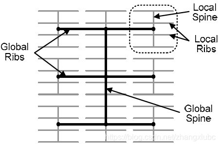
- From the center of the chip, all Wglobal clocks are distributed to the center of all regions using an spine-and-ribs distribution network with ny_region ribs, as shown below (H-tree).
- There is one local clock network per region. We denote the number of local clocks per region as Wlocal. The Wlocal signals are selected from the two sides of the FPGA that are closest to the region, devided evenly. skew beteen regions is not as important, since global clocks will likely be used if a clock is to drive multiple regions.
2nd network stage:
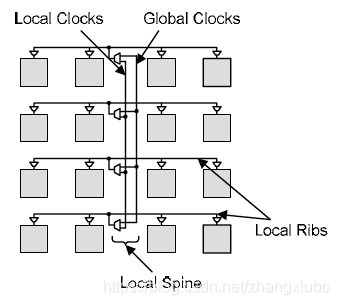
- The second network stage programmably connects clock signals from the center of each region to the logic blocks within that region. There is one of these networks for each region. The input to each second stage network consists of Wglobal global clocks and Wlocal local clocks from the first stage described above. These clocks are distributed using a spine-and-ribs topology. The spine contains Wglobal+Wlocal wires. In each row, a concentrator network is used to select any set of Wrib clocks from the spine. These clocks are distributed to the logic blocks in that row through a local rib. Each logic block in the row connects to the rib through another concentrator network; the concentrator is used to select any set of Wlb clocks from the rib.
3rd network stage:
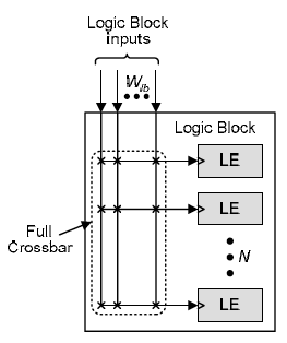
- The third network stage programmably connects the Wlb logic block clocks to the N logic elements within the logic block.
summary:
At the logic blocks, the incremental area cost of increasing the number of logic block clock inputs (Wlb) is large when Wlb < Wrib/2 but is small when Wlb > Wrib/2. For power, the number of used clocks in each logic block is far more important that than the number clocks that are available.
At the ribs, the area cost of increasing the number of clocks in each rib (Wrib) is large and dominated by the area of the rib-to-logic block switches. For power, the number of clocks that are used in each rib to be far more important than the number of clocks that are available.
At the spines, the area and power costs of increasing the number of clocks in each spine (Wspine) is not significant compared to that of increasing Wlb and Wrib.
Finally, increasing the number of the clock regions generally decreases area and power by reducing the number of clocks required in each region.


 1788
1788

 被折叠的 条评论
为什么被折叠?
被折叠的 条评论
为什么被折叠?
 到【灌水乐园】发言


