


方法一 :
全加器的逻辑电路图如下:
这个方法是通过两个半加器组成的
Verilog HDL代码如下:
module full_adder(
input wire A,
input wire B,
output wire C,
output wire sum
);

wire sum_h1;
wire count_h1;
wire count_h2;

half_adder half_adder1(
.A(A),
.B(B),
.sum(sum_h1),
.C(count_h1)
);

half_adder half_adder2(
.A(sum_h1),
.B(cin),
.sum(sum),
.C(count_h2)
);
assign C = count_h1 | count_h2;
endmodule 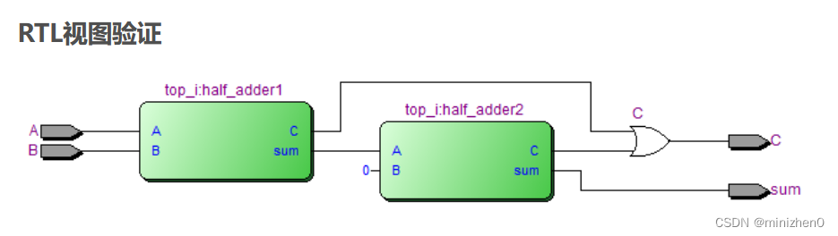
方法二:
直接求解全加器
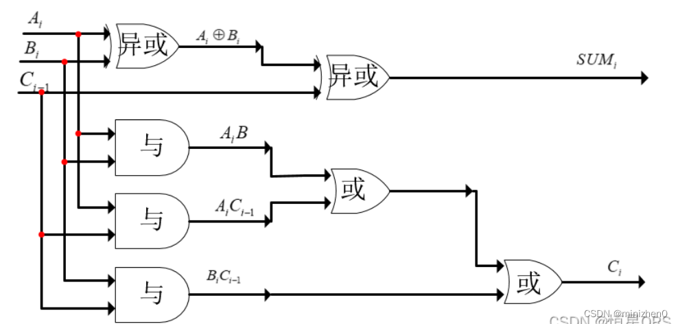
Verilog HDL代码如下:
module one_bit_full_adder(
input wire a,
input wire b,
input wire carry_in,
output wire sum,
output wire carry_out
);
assign sum = a ^ b ^ carry_in;
assign carry_out = (a & b) | (carry_in & (a ^ b));
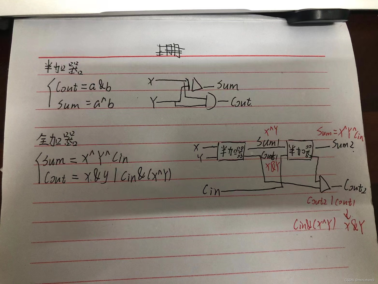
endmodule附加一个半加器代码,逻辑图在第一张图里有
module half adder(
	input wire A,
	input wire B,
	output wire C,
	output wire sum
);

//assign sum = (A == B) ? 0 : 1;  //这两种方式都可以实现
assign sum = A^B;
assign C= A&B;

endmodule
给四位全加器留一个位置稍后再更


 7081
7081

 被折叠的 条评论
为什么被折叠?
被折叠的 条评论
为什么被折叠?
 到【灌水乐园】发言


