关于引脚复用,不得不提的GPIO_Pin_sources 和GPIO_Pin

本文详细介绍了STM32中GPIO_Pin和GPIO_PinSource的区别,指出GPIO_Pin用于配置端口的基本属性,而GPIO_PinSource用于配置端口的复用功能。在STM32官方库中,这两个参数的定义不同,易引起混淆,作者提醒开发者注意区分。为避免配置问题,建议使用STM32CUBE库进行开发。

今天在端口复用时遇到了困惑,参考:http://www.51hei.com/bbs/dpj-40992-1.html


调整前的代码
GPIO_PinAFConfig(GPIOA,GPIO_Pin_9,GPIO_AF_4);
GPIO_PinAFConfig(GPIOA,GPIO_Pin_10,GPIO_AF_4);

调整后的代码
GPIO_PinAFConfig(GPIOA,GPIO_PinSource9,GPIO_AF_4);
GPIO_PinAFConfig(GPIOA,GPIO_PinSource10,GPIO_AF_4);


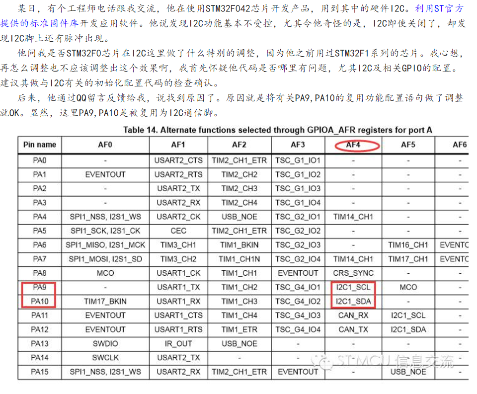
不难看出,该工程师调整的就是上面红色参数部分。一个是GPIO_Pin_N,一个是GPIO_PinSourceN,其实这2个参数是不一样的。


GPIO_Pin_n可以理解为某端口脚在整个端口的位置。比方某GPIO口的第6管脚位置编码GPIO_Pin_6 被定义为 ((uint16_t)0x0040) ,在对相应GPIO管脚做基本属性配置时会用到,如配置输入输出模式、模拟输入模式的选择等。有兴趣的话,可以点击GPIO_Init( )进去看看。


而GPIO_PinSourceN一般是在对某GPIO口相应pin脚的复用功能进行选择配置才会用到。它是根据端口各脚位的位置按顺序从0开始依次递增编号,可以理解为该管脚在该端口的序号。比方某GPIO口的第6号复用功能脚的序号GPIO_PinSource6 被定义为 ((uint8_t)0x06) 。有兴趣的话,也可以打开GPIO_PinAFConfig( )函数看看。显然,GPIO_PinSource6跟上面的GPIO_Pin_6的值相差甚远。


下面是ST官方库代码中有关GPIO_Pin_N的定义:


#define GPIO_Pin_0 ((uint16_t)0x0001)

#define GPIO_Pin_1 ((uint16_t)0x0002)

#define GPIO_Pin_2 ((uint16_t)0x0004)

#define GPIO_Pin_3 ((uint16_t)0x0008)

#define GPIO_Pin_4 ((uint16_t)0x0010)

#define GPIO_Pin_5 ((uint16_t)0x0020)

#define GPIO_Pin_6 ((uint16_t)0x0040)

#define GPIO_Pin_7 ((uint16_t)0x0080)

#define GPIO_Pin_8 ((uint16_t)0x0100)

#define GPIO_Pin_9 ((uint16_t)0x0200)

#define GPIO_Pin_10 ((uint16_t)0x0400)

。。。。。。

#define GPIO_Pin_15 ((uint16_t)0x8000)

#define GPIO_Pin_All ((uint16_t)0xFFFF)


下面是有关GPIO_PinSourceN的定义:

#define GPIO_PinSource0 ((uint8_t)0x00)

#define GPIO_PinSource1 ((uint8_t)0x01)

#define GPIO_PinSource2 ((uint8_t)0x02)

#define GPIO_PinSource3 ((uint8_t)0x03)

#define GPIO_PinSource4 ((uint8_t)0x04)

#define GPIO_PinSource5 ((uint8_t)0x05)

#define GPIO_PinSource6 ((uint8_t)0x06)

#define GPIO_PinSource7 ((uint8_t)0x07)

#define GPIO_PinSource8 ((uint8_t)0x08)

#define GPIO_PinSource9 ((uint8_t)0x09)

#define GPIO_PinSource10 ((uint8_t)0x0A)

。。。。。。

#define GPIO_PinSource15 ((uint8_t)0x0F)


小结:上面的问题只有基于STM32官方固件库开发时才会碰到。说实在的,这两个参数的确容易让人误解成一个东西或者弄混淆,尤其刚接触的人。经常有人在这个地方遇到麻烦,之前我在一篇文章中提到过。这里再特意提醒下。

不过ST官方后来推出的STM32CUBE库在这个地方的代码写法做了调整,不再定义GPIO_PinSourceN。当然,因为管脚配置导致异常的问题时有发生,建议使用ST官方推出的STM32CUBE配置环境及CUBE参考固件库着手开发,这样会省不少事。

软件SPI替换成为硬件SPI 只需要修改SPI相关部分 ads1256.h中的 “寄存器地址”“命令定义”不可以更改 你只需要修改SPI的配置读写使代码能够完成STM32F407硬件SPI1读取ADS1256模块采集的数据 #include "stm32f4xx.h" #include "ads1256.h" #include "delay.h" #include "stm32f4xx_it.h" #include "stm32f4xx_rcc.h" #include "stm32f4xx_exti.h" // int32_t AdcNow[8]; // 8路ADC采集结果(实时)有符号数 // uint8_t Channel; // 当前通道 // uint8_t ScanMode; // 扫描模式,0表示单端8路, 1表示差分4路 /********************************************************************************************************* * 函 数 名: ADS1256_GPIO_Init * 功能说明: ADC GPIO初始化 * 形 参: 无 * 返 回 值: 无 *********************************************************************************************************/ void ADS1256_GPIO_Init(void) { GPIO_InitTypeDef GPIO_InitStructure; // 模式103gpio口配置为注释部分 /* GPIOF Periph clock enable */ // RCC_APB2PeriphClockCmd(RCC_APB2Periph_GPIOD | RCC_APB2Periph_AFIO, ENABLE); RCC_AHB1PeriphClockCmd(RCC_AHB1Periph_GPIOD, ENABLE); RCC_APB2PeriphClockCmd(RCC_APB2Periph_SYSCFG, ENABLE);//?????SYSCFG?? // GPIO_InitStructure.GPIO_Pin = GPIO_Pin_0 | GPIO_Pin_1 | GPIO_Pin_4 | GPIO_Pin_5; // GPIO_InitStructure.GPIO_Mode = GPIO_Mode_Out_PP; // GPIO_InitStructure.GPIO_Speed = GPIO_Speed_50MHz; GPIO_InitStructure.GPIO_Pin = GPIO_Pin_0 | GPIO_Pin_1 | GPIO_Pin_4 | GPIO_Pin_5 | GPIO_Pin_6; GPIO_InitStructure.GPIO_Mode = GPIO_Mode_OUT; GPIO_InitStructure.GPIO_Speed = GPIO_Fast_Speed; GPIO_InitStructure.GPIO_OType = GPIO_OType_PP; GPIO_InitStructure.GPIO_PuPd = GPIO_PuPd_NOPULL; GPIO_Init(GPIOD, &GPIO_InitStructure); // GPIO_InitStructure.GPIO_Pin = GPIO_Pin_2; // GPIO_InitStructure.GPIO_Mode = GPIO_Mode_IN_FLOATING; // GPIO_InitStructure.GPIO_Speed = GPIO_Speed_50MHz; GPIO_InitStructure.GPIO_Pin = GPIO_Pin_2; GPIO_InitStructure.GPIO_Mode = GPIO_Mode_IN; GPIO_InitStructure.GPIO_Speed = GPIO_Fast_Speed; GPIO_InitStructure.GPIO_PuPd = GPIO_PuPd_NOPULL; GPIO_Init(GPIOD, &GPIO_InitStructure); // GPIO_InitStructure.GPIO_Pin = GPIO_Pin_3; // GPIO_InitStructure.GPIO_Mode = GPIO_Mode_IPD; // GPIO_InitStructure.GPIO_Speed = GPIO_Speed_50MHz; GPIO_InitStructure.GPIO_Pin = GPIO_Pin_3; GPIO_InitStructure.GPIO_Mode = GPIO_Mode_IN; GPIO_InitStructure.GPIO_Speed = GPIO_Fast_Speed; GPIO_InitStructure.GPIO_PuPd = GPIO_PuPd_DOWN; GPIO_Init(GPIOD, &GPIO_InitStructure); RST_L; // 拉低复位引脚 delay_ms(1); RST_H; // 拉高复位引脚 delay_ms(100); CS_H; // 拉高片选引脚 SCLK_L; // 拉低时钟引脚 DIN_H; // 拉高输入引脚 } /* ********************************************************************************************************* * 函 数 名: ADS1256_Send8Bit * 功能说明: 向SPI总线发送8个bit数据。 不带CS控制。 * 形 参: _data : 数据 * 返 回 值: 无 ********************************************************************************************************* */ void ADS1256_Send8Bit(uint8_t data) { uint8_t i; /* 连续发送多个字节时,需要延迟一下 */ delay_us(1); /* ADS1256 要求 SCL高电平低电平持续时间最小 200ns */ for(i = 0; i < 8; i++) { if (data & 0x80) { DIN_H; } else { DIN_L; } SCLK_H; delay_us(1); data <<= 1; SCLK_L; /* <---- ADS1256 是在SCK下降沿采样DIN数据, 数据必须维持 50nS */ delay_us(1); } } /********************************************************************************************************* * 函 数 名: ADS1256_Recive8Bit * 功能说明: 从SPI总线接收8个bit数据。 不带CS控制。 * 形 参: 无 * 返 回 值: 无 *********************************************************************************************************/ uint8_t ADS1256_Recive8Bit(void) { uint8_t i; uint8_t read = 0; Delay_ns(250); Delay_ns(250); Delay_ns(250); Delay_ns(250); /* ADS1256 要求 SCL高电平低电平持续时间最小 200ns */ for (i = 0; i < 8; i++) { SCLK_H; Delay_ns(250); Delay_ns(250); read = read<<1; SCLK_L; if (DO_IS_H) { read++; } Delay_ns(250); Delay_ns(250); } return read; } /********************************************************************************************************* * 函 数 名: ADS1256_WriteReg * 功能说明: 写指定的寄存器 * 形 参: _RegID : 寄存器ID * _RegValue : 寄存器值 * 返 回 值: 无 *********************************************************************************************************/ void ADS1256_WriteReg(uint8_t RegID, uint8_t RegValue) { CS_L; /* SPI片选 = 0 */ ADS1256_Send8Bit(CMD_WREG | RegID); /* 写寄存器的命令, 并发送寄存器地址 */ ADS1256_Send8Bit(0x00); /* 寄存器个数 - 1, 此处写1个寄存器 */ ADS1256_Send8Bit(RegValue); /* 发送寄存器值 */ CS_H; /* SPI片选 = 1 */ } /********************************************************************************************************* * 函 数 名: ADS1256_ReadReg * 功能说明: 读指定的寄存器 * 形 参: _RegID : 寄存器ID * _RegValue : 寄存器值。 * 返 回 值: 读到的寄存器值。 *********************************************************************************************************/ uint8_t ADS1256_ReadReg(uint8_t _RegID) { uint8_t read; CS_L; /* SPI片选 = 0 */ ADS1256_Send8Bit(CMD_RREG | _RegID); /* 写寄存器的命令, 并发送寄存器地址 */ ADS1256_Send8Bit(0x00); /* 寄存器个数 - 1, 此处读1个寄存器 */ delay_us(1); /* 必须延迟才能读取芯片返回数据 */ read = ADS1256_Recive8Bit(); /* 读寄存器值 */ CS_H; /* SPI片选 = 1 */ return read; } /********************************************************************************************************* * 函 数 名: ADS1256_WriteCmd * 功能说明: 发送单字节命令 * 形 参: _cmd : 命令 * 返 回 值: 无 *********************************************************************************************************/ void ADS1256_WriteCmd(uint8_t cmd) { CS_L; /* SPI片选 = 0 */ ADS1256_Send8Bit(cmd); CS_H; /* SPI片选 = 1 */ } //----------------------------------------------------------------- // void ADS1256_CfgADC(unsigned char gain,unsigned char drate) //----------------------------------------------------------------- // 函数功能: 配置ADC参数,增益及转换速率 // 入口参数: 增益,速率 // 返回参数: 无 // 全局变量: 无 // 调用模块: void ADS1256_WriteCmd(unsigned char cmd) // void ADS1256_WriteReg(unsigned char Reg_ID,unsigned char Reg_Date) // void ADS1256_Send8Bit(unsigned char date) // 注意事项: //----------------------------------------------------------------- void ADS1256_CfgADC(uint8_t gain,uint8_t drate) // 初始化设置,设置增益以及转换速率 { ADS1256_WriteCmd(CMD_RESET); // 写复位指令 ADS1256_WriteReg(REG_STATUS,0XF4); // 写状态,数据传输默认高位在前,启动矫正,禁止使用缓冲 ADS1256_WriteCmd(CMD_SELFCAL); // 自校准 delay_us(200); { uint8_t buf[4]; /* 状态寄存器定义 Bits 7-4 ID3, ID2, ID1, ID0 Factory Programmed Identification Bits (Read Only) Bit 3 ORDER: Data Output Bit Order 0 = Most Significant Bit First (default) 1 = Least Significant Bit First Input data is always shifted in most significant byte and bit first. Output data is always shifted out most significant byte first. The ORDER bit only controls the bit order of the output data within the byte. Bit 2 ACAL : Auto-Calibration 0 = Auto-Calibration Disabled (default) 1 = Auto-Calibration Enabled When Auto-Calibration is enabled, self-calibration begins at the completion of the WREG command that changes the PGA (bits 0-2 of ADCON register), DR (bits 7-0 in the DRATE register) or BUFEN (bit 1 in the STATUS register) values. Bit 1 BUFEN: Analog Input Buffer Enable 0 = Buffer Disabled (default) 1 = Buffer Enabled Bit 0 DRDY : Data Ready (Read Only) This bit duplicates the state of the DRDY pin. ACAL=1使能自校准功能。当 PGA,BUFEEN, DRATE改变时会启动自校准 */ buf[0] = (0 << 3) | (1 << 2) | (1 << 1); /* 高四位0表示AINP接 AIN0, 低四位8表示 AINN 固定接 AINCOM */ buf[1] = 0x01; //通道设置选择 /* ADCON: A/D Control Register (Address 02h) Bit 7 Reserved, always 0 (Read Only) Bits 6-5 CLK1, CLK0 : D0/CLKOUT Clock Out Rate Setting 00 = Clock Out OFF 01 = Clock Out Frequency = fCLKIN (default) 10 = Clock Out Frequency = fCLKIN/2 11 = Clock Out Frequency = fCLKIN/4 When not using CLKOUT, it is recommended that it be turned off. These bits can only be reset using the RESET pin. Bits 4-2 SDCS1, SCDS0: Sensor Detect Current Sources 00 = Sensor Detect OFF (default) 01 = Sensor Detect Current = 0.5 μ A 10 = Sensor Detect Current = 2 μ A 11 = Sensor Detect Current = 10μ A The Sensor Detect Current Sources can be activated to verify the integrity of an external sensor supplying a signal to the ADS1255/6. A shorted sensor produces a very small signal while an open-circuit sensor produces a very large signal. Bits 2-0 PGA2, PGA1, PGA0: Programmable Gain Amplifier Setting 000 = 1 (default) 001 = 2 010 = 4 011 = 8 100 = 16 101 = 32 110 = 64 111 = 64 */ buf[2] = (0 << 5) | (0 << 3) | (gain << 0); buf[3] = drate; // DRATE_10SPS; /* 选择数据输出速率 */ CS_L; ADS1256_Send8Bit(CMD_WREG|0); // 写寄存器 ADS1256_Send8Bit(0x03); // 连续写入4个数据 ADS1256_Send8Bit(buf[0]); // 设置状态寄存器 ADS1256_Send8Bit(buf[1]); // 设置输入通道参数 ADS1256_Send8Bit(buf[2]); // 设置ADCON控制寄存器,增益 ADS1256_Send8Bit(buf[3]); // 设置数据速率 CS_H; } delay_us(50); } //----------------------------------------------------------------- // unsigned long ADS1256_GetAdc(unsigned char channel) //----------------------------------------------------------------- // 函数功能: 获取ADC的采样结果 // 入口参数: 无 // 返回参数: ADC采样结果 // 全局变量: 无 // 调用模块: void ADS1256_WriteCmd(unsigned char cmd) // void ADS1256_WriteReg(unsigned char Reg_ID,unsigned char Reg_Date) // void ADS1256_Send8Bit(unsigned char date) // 注意事项: //----------------------------------------------------------------- uint32_t ADS1256_GetAdc(uint8_t channel) { uint32_t read; read = 0; // while(DRDY); //当DRDY变为低电平时,数据开始传输 delay_us(5); ADS1256_WriteReg(REG_MUX,channel); // 写入读取的通道 ADS1256_WriteCmd(CMD_SYNC); //同步A/D转换命令 delay_us(5); ADS1256_WriteCmd(CMD_WAKEUP); //完成SYNC并退出待机模式 while(!DRDY_IS_L); // 等待数据转换完成 CS_L; //片选拉低 ADS1256_Send8Bit(CMD_RDATA); //读取数据命令 delay_us(2); //连续接收3个数据,高字节在前 read = ((uint32_t)ADS1256_Recive8Bit() << 16); read +=( (uint32_t)ADS1256_Recive8Bit() << 8); read += ADS1256_Recive8Bit() ; delay_us(2); // read=0x678965; return read; } float ADS1256_GetAdc_V(uint8_t channel) { uint32_t read,reads; read = 0; float V; // while(DRDY); //当DRDY变为低电平时,数据开始传输 delay_us(5); ADS1256_WriteReg(REG_MUX,channel); // 写入读取的通道 ADS1256_WriteCmd(CMD_SYNC); //同步A/D转换命令 delay_us(5); ADS1256_WriteCmd(CMD_WAKEUP); //完成SYNC并退出待机模式 while(!DRDY_IS_L); // 等待数据转换完成 CS_L; //片选拉低 ADS1256_Send8Bit(CMD_RDATA); //读取数据命令 delay_us(2); //连续接收3个数据,高字节在前 read = ((uint32_t)ADS1256_Recive8Bit() << 16); read +=( (uint32_t)ADS1256_Recive8Bit() << 8); read += ADS1256_Recive8Bit() ; delay_us(2); CS_H; reads = (read ^ 0x800000); V=(((0.596047*reads)-5000000)/1000000); // read=0x678965; return V; } #ifndef _ads1256_H #define _ads1256_H #include "stm32f4xx.h" /* 寄存器地址, 后面是复位后缺省值 */ #define REG_STATUS (0) // x1H 状态寄存器 #define REG_MUX (1) // 01H 输入多路复用器控制寄存器 #define REG_ADCON (2) // 20H A/D控制寄存器 #define REG_DRATE (3) // F0H A/D数据速率 #define REG_IO (4) // E0H GPIO控制寄存器 #define REG_OFC0 (5) // xxH 偏移校准字节0,最低有效字节 #define REG_OFC1 (6) // xxH 偏移校准字节1 #define REG_OFC2 (7) // xxH 偏移校准字节2,最高有效字节 #define REG_FSC0 (8) // xxH 满量程校准字节0,最低有效字节 #define REG_FSC1 (9) // xxH 满量程校准字节1 #define REG_FSC2 (10)// xxH 满量程校准字节2,最高有效字节 /* 命令定义: TTable 24. Command Definitions --- ADS1256数据手册第34页 */ #define CMD_WAKEUP (0x00) // Completes SYNC and Exits Standby Mode 0000 0000 (00h) 完成SYNC并退出待机状态 #define CMD_RDATA (0x01) // Read Data 0000 0001 (01h) 读取数据 #define CMD_RDATAC (0x03) // Read Data Continuously 0000 0011 (03h) 连续读取数据 #define CMD_SDATAC (0x0F) // Stop Read Data Continuously 0000 1111 (0Fh) 停止连续读取数据 #define CMD_RREG (0x10) // Read from REG rrr 0001 rrrr (1xh) 从REG读取 #define CMD_WREG (0x50) // Write to REG rrr 0101 rrrr (5xh) 写到REG #define CMD_SELFCAL (0xF0) // Offset and Gain Self-Calibration 1111 0000 (F0h) 偏移增益自校准 #define CMD_SELFOCAL (0xF1) // Offset Self-Calibration 1111 0001 (F1h) 偏移自校准 #define CMD_SELFGCAL (0xF2) // Gain Self-Calibration 1111 0010 (F2h) 增益自校准 #define CMD_SYSOCAL (0xF3) // System Offset Calibration 1111 0011 (F3h) 系统偏移校准 #define CMD_SYSGCAL (0xF4) // System Gain Calibration 1111 0100 (F4h) 系统增益校准 #define CMD_SYNC (0xFC) // Synchronize the A/D Conversion 1111 1100 (FCh) 同步A/D转换 #define CMD_STANDBY (0xFD) // Begin Standby Mode 1111 1101 (FDh) 开始待机模式 #define CMD_RESET (0xFE) // Reset to Power-Up Values 1111 1110 (FEh) 重置为开机值 #define PGA_1 0x00 #define PGA_2 0x01 #define PGA_4 0x02 #define PGA_8 0x03 #define PGA_16 0x04 #define PGA_32 0x05 #define PGA_64 0x06 #define POSITIVE_AIN0 (0X00) #define POSITIVE_AIN1 (0X10) #define POSITIVE_AIN2 (0X20) #define POSITIVE_AIN3 (0X30) #define POSITIVE_AIN4 (0X40) #define POSITIVE_AIN5 (0X50) #define POSITIVE_AIN6 (0X60) #define POSITIVE_AIN7 (0X70) #define POSITIVE_AINCOM (0X80) #define NEGTIVE_AIN0 0X00 #define NEGTIVE_AIN1 0X01 #define NEGTIVE_AIN2 0X02 #define NEGTIVE_AIN3 0X03 #define NEGTIVE_AIN4 0X04 #define NEGTIVE_AIN5 0X05 #define NEGTIVE_AIN6 0X06 #define NEGTIVE_AIN7 0X07 #define NEGTIVE_AINCOM 0X08 #define DATARATE_30K 0xF0 #define DATARATE_15K 0xE0 #define DATARATE_7_5K 0xD0 #define DATARATE_3_7_5K 0xC0 #define DATARATE_2K 0xB0 #define DATARATE_1K 0xA0 #define DATARATE_500 0x92 #define DATARATE_100 0x82 #define DATARATE_60 0x72 #define DATARATE_50 0x63 #define DATARATE_30 0x53 #define DATARATE_25 0x43 #define DATARATE_15 0x33 #define DATARATE_10 0x23 #define DATARATE_5 0x13 #define DATARATE_2_5 0x02 #define SET (GPIOD,GPIO_Pin_6) #define SET_L GPIO_ResetBits(GPIOD,GPIO_Pin_6) #define SET_H GPIO_SetBits(GPIOD,GPIO_Pin_6) #define RST (GPIOD,GPIO_Pin_5) #define RST_L GPIO_ResetBits(GPIOD,GPIO_Pin_5) #define RST_H GPIO_SetBits(GPIOD,GPIO_Pin_5) #define CS (GPIOD,GPIO_Pin_4) #define CS_L GPIO_ResetBits(GPIOD,GPIO_Pin_4) #define CS_H GPIO_SetBits(GPIOD,GPIO_Pin_4) #define DRDY (GPIOD,GPIO_Pin_3) #define DRDY_L GPIO_ResetBits(GPIOD,GPIO_Pin_3) #define DRDY_H GPIO_SetBits(GPIOD,GPIO_Pin_3) #define DRDY_IS_L (GPIO_ReadInputDataBit(GPIOD,GPIO_Pin_3) == Bit_RESET) #define DOUT (GPIOD,GPIO_Pin_2) #define DOUT_L GPIO_ResetBits(GPIOD,GPIO_Pin_2) #define DOUT_H GPIO_SetBits(GPIOD,GPIO_Pin_2) #define DO_IS_H (GPIO_ReadInputDataBit(GPIOD,GPIO_Pin_2) == Bit_SET) #define DIN (GPIOD,GPIO_Pin_1) #define DIN_L GPIO_ResetBits(GPIOD,GPIO_Pin_1) #define DIN_H GPIO_SetBits(GPIOD,GPIO_Pin_1) #define SCLK (GPIOD,GPIO_Pin_0) #define SCLK_L GPIO_ResetBits(GPIOD,GPIO_Pin_0) #define SCLK_H GPIO_SetBits(GPIOD,GPIO_Pin_0) ///*STATUS REGISTER*/ //#define MSB_FRIST (0x00<<3) //#define LSB_FRIST (0x01<<3) //#define ACAL_OFF (0x00<<2) //#define ACAL_ON (0x01<<2) //#define BUFEN_OFF (0x00<<1) //#define BUFEN_ON (0x01<<1) ///*ADCON REGISTER*/ //#define CLKOUT_OFF (0x00<<5) //#define CLKOUT_CLKIN (0x01<<5) //#define DETECT_OFF (0x00<<3) //#define DETECT_ON_2UA (0x02<<3) uint32_t ADS1256_GetAdc(uint8_t channel); float ADS1256_GetAdc_V(uint8_t channel); void ADS1256_CfgADC(uint8_t gain,uint8_t drate); void ADS1256_GPIO_Init(void); #endif
最新发布
08-21
评论
添加红包

请填写红包祝福语或标题

红包个数最小为10个

红包金额最低5元

当前余额3.43前往充值 >
需支付:10.00
成就一亿技术人!
领取后你会自动成为博主和红包主的粉丝 规则
hope_wisdom
发出的红包
实付
使用余额支付
点击重新获取
扫码支付
钱包余额 0

抵扣说明:

1.余额是钱包充值的虚拟货币,按照1:1的比例进行支付金额的抵扣。
2.余额无法直接购买下载,可以购买VIP、付费专栏及课程。

余额充值