


 本文介绍了使用DSP28335开发板进行LED灯闪烁的实践过程,涉及JTAG接口的EMU0和EMU1信号功能,以及GPIO的配置和寄存器使用。通过编译工程并分析代码,揭示了库函数如何控制GPIO实现LED的开关,并提及了部分汇编指令的应用。
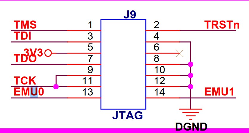
1. 本次以三兄弟的DSP28335开发板为例,看下JTAG接口,EMU0,EMU1的用途,不是很懂,不深入研究,用到再说
EMU0/1是TI芯片的JTAG才有的信号,本身不属于JTAG标准里的信号,有两个作用。
(1)设定芯片是仿真模式(上拉)还是边界扫描模式(下拉)。
(2)用做高速实时数据交换RTDX及TRACE等功能时。这个一般用户可能用不到。
所以这两个信号是双向的,这个信号一般来说不需加要buffer,直接连起来就好了,不用管他是单向还是双向。
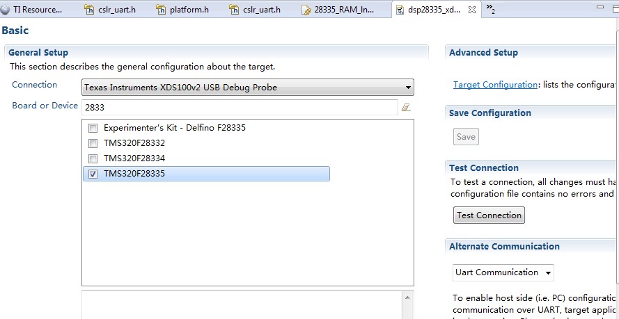
2. 打开工程,E:\dsp\SXD_C28335\SXD28335_PRO_1_V2\Example_2833x_LEDBlink,建立一个CCXML文件,编译一下工程
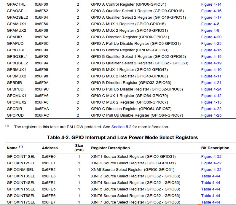
3. 看下引脚原理图,28335有3组GPIO,每组GPIO最多有32个引脚,但是28335是16位的,所以每组GPIO有高低寄存器

4. GPIO寄存器
5. 代码研究一下,看了一下底层用的是C2000WARE里面的库函数。
  1 #include "DSP28x_Project.h"     // Device Headerfile and Examples Include File
  2
  3 // Prototype statements for functions found within this file.
  4 interrupt void cpu_timer0_isr(void);
  5
  6 void main(void)
  7 {
  8
  9 // Step 1. Initialize System Control:
 10 // PLL, WatchDog, enable Peripheral Clocks
 11 // This example function is found in the DSP2833x_SysCtrl.c file.
 12    InitSysCtrl();
 13
 14 // Step 2. Initalize GPIO:
 15 // This example function is found in the DSP2833x_Gpio.c file and
 16 // illustrates how to set the GPIO to it's default state.
 17 // InitGpio();  // Skipped for this example
 18
 19
 20 // Step 3. Clear all interrupts and initialize PIE vector table:
 21 //
 最低0.47元/天 解锁文章


 1696
1696

 被折叠的 条评论
为什么被折叠?
被折叠的 条评论
为什么被折叠?
 到【灌水乐园】发言


