


在使用sentaurus TCAD的过程中,我们往往需要调试最后sdevice跑出来的Ion和Ioff大小。
调Ion和Ioff的目的:
1. 得到更好的器件性能;
2. 和实验中/文献中的IV曲线对上;
调Ion和Ioff的思路:
从影响因素上看,往往可以从器件的几何结构,器件掺杂和物理模型三个方面讨论。
从调试思路上看,为了校准IV,可以先调IV的shape,再校准Ioff,最后校准Ion。
调Ion和Ioff的具体过程记录:
步骤一:用sde搭建器件
这里,我们以bulk CMOS为例。首先用sde搭建一个几何模型,如图所示:
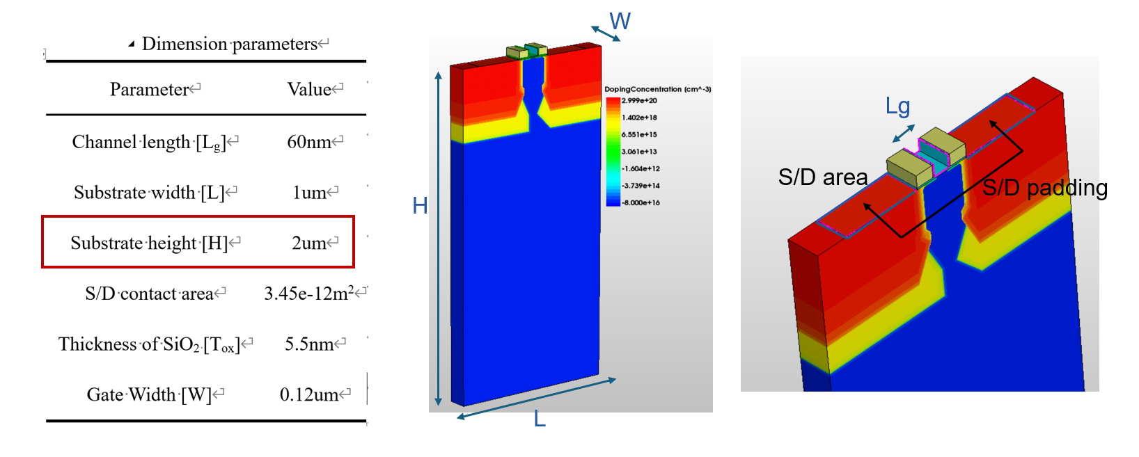 具体实现代码如下:(其中包含了许多可以调整的几何参数,有兴趣的同学可以自己设置)
; Reinitializing SDE
(sde:clear)

;Height of substrate
(define  Hsub @Hsub@);1
(display "Height of substate: ") (display Hsub) (display "um")
(newline)
;Height of spacer
(define  Hsp  @Hsp@);0.1
(display "Height of spacer : ") (display Hsp) (display "um")
(newline)
;Length of total
(define  Lsub @Lsub@);1
(display "Length of substrate: ") (display Lsub) (display "um")
(newline)
;Length of gate
(define  Lg @Lg@);0.06
(display "Length of gate: ") (display Lg) (display "um")
(newline)
;Length of spacer
(define  Lsp @Lsp@);0.2
(display "Length of pacer: ") (display Lsp) (display "um")
(newline)


;Length of oxide
(define  Lox @Lox@);0.2
(display "Length of ox: ") (display Lox) (display "um")
(newline)

;oxide
(define  Tox @Tox@);0.04
(display "Thickness of oxide: ") (display Tox) (display "um")
(newline)

;W
(define  W @W@);
(display "Width: ") (display W) (display "um")
(newline)


(define Xsub (/ Lsub 2.0))
(define Ysub  Hsub)

(define Xsp (/ Lsp 2.0))

(define Xox (/ Lox 2.0))

(define Xg (/ Lg 2.0))

; set coordinate system up direction
(sde:set-process-up-direction "+z")

; Selecting default Boolean expression
(sdegeo:set-default-boolean "ABA")

; Creating rectangular regions
(sdegeo:create-cuboid
  (position (- Xsub)  0  0.0) (position Xsub  Ysub   W)
  "Silicon" "substrate"
)

(sdegeo:create-cuboid
  (position (- Xox) (- Tox) 0.0) (position Xox  0.0   W)
  "Oxide" "R.Gateox"
)

(sdegeo:create-cuboid
  (position (- Xsp) (- Hsp)   0.0) (position Xsp (- Tox) W)
  "Nitride" "R.Spacer"
)

(define  Tox2 @Tox2@);0.0002
(sdegeo:create-cuboid
  (position (- (- Xg) Tox2) (- Hsp)   0.0) (position (+ Xg Tox2) (- Tox) W)
  "Oxide" "R.Gateox2"
)
(sdegeo:create-cuboid
  (position (- Xg) (- Hsp)  0.0) (position  Xg (- Tox) W)
  "Nitride" "R.Polygate"
)

(sdegeo:create-cuboid
  (position (+ Xox 0.285) 0  0.0) (position  (+ Xox 0.002) 0.001 W)
  "Silicon" "R.del1"
)
(sdegeo:create-cuboid
  (position (- (- Xox) 0.285) 0  0.0) (position  (- (- Xox) 0.002) 0.001 W)
  "Silicon" "R.del2"
)
(sdegeo:set-contact (find-body-id (position (+ Xox 0.1) 0.0005 (/ W 2))) "C.drain" "remove")
(sdegeo:set-contact (find-body-id (position (- (- Xox) 0.1)  0.0005 (/ W 2))) "C.source" "remove")

;(sdegeo:delete-region(find-body-id (position (+ Xox 0.1) 0.0005 (/ W 2) )))
; Rounding edges
;(sde:define-parameter "fillet-radius" 0.08 0.0 0.0 )
;(sdegeo:fillet-2d (find-vertex-id (position -0.2 -0.2 0.0)) fillet-radius)
;(sdegeo:fillet-2d (find-vertex-id (position  0.2 -0.2 0.0)) fillet-radius)

; Defining contacts

;(sdegeo:set-current-contact-set "C.source")
;(sdegeo:set-contact (find-face-id (position (- (- Xox) 0.05)  0 (/ W 2))) "C.source")

;(sdegeo:set-current-contact-set "C.drain")
;(sdegeo:set-contact (find-face-id (position (+  Xox 0.05)  0.0 (/ W 2)))  "C.drain")


;(sdegeo:set-contact (find-face-id  (position 0.0 (- Hsp) (/ W 2))) "gate" )
(sdegeo:set-contact (find-face-id (position  0.0  Hsub (/ W 2))) "C.substrate")
(sdegeo:set-contact (find-body-id (position 0.0 (- Hsp) (/ W 2))) "gate" "remove")


; Constant doping profile definions
(sdedr:define-constant-profile "Const.Bulk" "BoronActiveConcentration" @d_bulk@)
(sdedr:define-constant-profile-region "PlaceCD.Bulk"
  "Const.Bulk" "substrate")

(sdedr:define-constant-profile "Const.Poly" "ArsenicActiveConcentration" @d_poly@)
(sdedr:define-constant-profile-region "PlaceCD.Poly"
  "Const.Poly" "R.Polygate")


(define  L_dop_sd_g @L_dop_sd_g@);0.01

; S/D Imp
(sdedr:define-refeval-window "BaseLine.Source" "cuboid"
 (position  (- (- Xg) L_dop_sd_g) @depth_sd@ 0.0)  (position (- Xsub) 0.0 W) )

(sdedr:define-refeval-window "BaseLine.Drain" "cuboid"
 (position (+ Xg L_dop_sd_g) @depth_sd@ 0.0)  (position Xsub  0.0 W) )

(sdedr:define-gaussian-profile "Gauss.SourceDrain"
  "ArsenicActiveConcentration" "PeakPos" 0.0 "PeakVal" @d_sd@
  "ValueAtDepth" (* 0.1 @d_sd@) "Depth" @dep_sd@ "Gauss" "Factor" @G_factor@)

(sdedr:define-analytical-profile-placement "PlaceAP.Source"
 "Gauss.SourceDrain" "BaseLine.Source" "Both" "NoReplace" "Eval")

(sdedr:define-analytical-profile-placement "PlaceAP.Drain"
 "Gauss.SourceDrain" "BaseLine.Drain" "Both" "NoReplace" "Eval")

(define  ldd_dop @ldd_dop@);1e19
(define  ldd_l @ldd_l@);0.01
(define  ldd_h @ldd_h@);0.01


#if @ADD_LDD@ == 1
 ;LDD Imp
(sdedr:define-refinement-window "ldd.Source" "cuboid"
 (position  (+ (- Xg) @ldd_l@) 0.0 0.0)  (position (- (- Xg) 0.05) @ldd_h@ W) )

(sdedr:define-refinement-window "ldd.Drain" "cuboid"
(position  (- Xg @ldd_l@)  0.0   0.0)  (position (+ Xg 0.05)  @ldd_h@  W) )

(sdedr:define-constant-profile "ldd" "ArsenicActiveConcentration" @ldd_dop@ )

(sdedr:define-constant-profile-placement "ldd-place" "ldd" "ldd.Drain")
(sdedr:define-constant-profile-placement "ldd-place1" "ldd" "ldd.Source")
#endif

; Meshing strategies
(sdedr:define-refeval-window "RefWin.Global" "cuboid"
    (position (- Xsub)  0  0.0) (position Xsub  Ysub   W) )

(sdedr:define-refinement-size "RefDef.Global"
  0.1  0.1
  0.04 0.04
0.08 0.08 )

(sdedr:define-refinement-placement "Place.Global"
 "RefDef.Global" "RefWin.Global" )


(sdedr:define-refeval-window "RefWin.Active" "cuboid"
 (position (- Xox) -0.2 0 ) (position Xox 0.2 W))
(sdedr:define-refinement-size "RefDef.Active"
  0.06  0.06
  0.05 0.05
 0.1 0.1 )

(sdedr:define-refinement-placement "Place.Active"
"RefDef.Active" "RefWin.Active")


(sdedr:define-refeval-window "RefWin.channel" "cuboid"
  (position (- (- Xox) 0.1) 0 0) (position (+ 0.1 Xox) 0.3 W))

(sdedr:define-refinement-size "RefDef.channel"
  @refine_size_max@  @refine_size_max@
  @refine_size_min@  @refine_size_min@
 0.1 0.1)

(sdedr:define-refinement-placement "Place.Global"
 "RefDef.channel" "RefWin.channel" )


; Saving the model
(sde:save-model "n@node@_geo")
; Build Mesh
(sde:build-mesh "n@node@_msh")
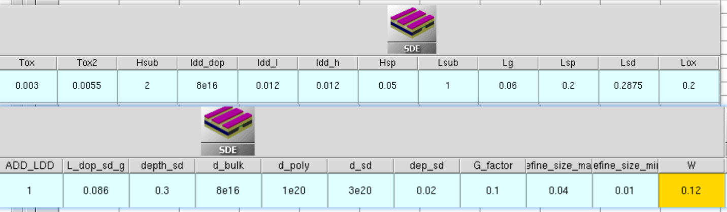
sde中参数设置如下
步骤二:用sdevice给器件电流仿真激励
#define _CAR1_    Electron

#define _DG_     eQuantumPotential
#define _Vdd_    @Vd@
#define _VdLin_  @Vg@

Electrode{
   { Name="C.source"    Voltage= 0.0 }
   { Name="C.drain"     Voltage= 0.0 }
   { Name="gate"       Voltage=0.0 Schottky Workfunction=@WF@}
   { Name="C.substrate"      Voltage= 0.0 }
}

File {
   Grid=   "@tdr@"
   Plot=   "@tdrdat@"
   Current="@plot@"
   Output= "@log@"
Parameter = "@parameter@"

}

Physics {
Fermi
Mobility (
PhuMob
Enormal( @Enormal@)
)

}


Plot{
*--Density and Currents, etc
VertexIndex
eJouleHeat
   eDensity hDensity
   TotalCurrent/Vector eCurrent/Vector hCurrent/Vector
   eMobility hMobility
   eVelocity hVelocity
   eQuasiFermi hQuasiFermi

*--Temperature
   eTemperature Temperature hTemperature

*--Fields and charges
   ElectricField/Vector Potential SpaceCharge

*--Doping Profiles
   Doping DonorConcentration AcceptorConcentration

*--Generation/Recombination
   SRH Band2Band * Auger
   * AvalancheGeneration eAvalancheGeneration hAvalancheGeneration

*--Driving forces
   eGradQuasiFermi/Vector hGradQuasiFermi/Vector
   eEparallel hEparallel eENormal hENormal

*--Band structure/Composition
   BandGap
   BandGapNarrowing
   Affinity
   ConductionBand ValenceBand
   eQuantumPotential hQuantumPotential

*--Stress related data
   StressXX StressYY StressZZ
   StressXY StressXZ StressYZ

}


Math {
  Extrapolate
  Derivatives
  RelErrControl
  Digits=5
  RHSmin=1e-10
  Notdamped=100
  Iterations=500
  DirectCurrent
  ExitOnFailure
  *Method=ParDiso
}

Solve{
  #-initial solution:
  NewCurrentPrefix="init_"
  Coupled(Iterations= 100 LineSearchDamping= 1e-4   ){ Poisson _DG_}
  Coupled { Poisson _CAR1_ _DG_ }

#----------------------------------------------------------------------#
#- IdVg
#if @IdVd@ == 0
#----------------------------------------------------------------------#


  #-ramp drain
  Quasistationary(
     InitialStep= 1e-7
     MaxStep= 0.1 Minstep= 1.e-15
     Increment= 1.3
     Goal { Name="C.drain" Voltage=@Vd@ }
  ){ Coupled{  Poisson _CAR_ _DG_} }

  NewCurrentPrefix="IdVg_VdLin_"
  #-ramp gate:
  Quasistationary(
     DoZero
     InitialStep= 1.e-8
     MaxStep= 0.01 Minstep= 1.e-15
     Increment= 1.3
     Goal{ Name="gate" Voltage=@Vg@ }
  ){ Coupled{  Poisson _CAR_ _DG_} }

#----------------------------------------------------------------------#
#- IdVd
#else
#----------------------------------------------------------------------#

 Quasistationary(
      InitialStep= 1e-3 Increment= 1.25
      Minstep= 1e-5 MaxStep= 0.2
      Goal{ Name="gate"  Voltage= 0 }
   ){ Coupled{ Poisson _CAR1_ _DG_ } }

   Quasistationary(
      InitialStep= 1e-3 Increment= 1.2
      Minstep= 1e-5 MaxStep= 0.2
      Goal{ Name="gate"  Voltage= @Vg@ }
   ){ Coupled{ Poisson _CAR1_ _DG_ }
      Save(
        FilePrefix="n@node@"
        Time=(Range=(0 1) Intervals= @<IdVd-1>@ )
        NoOverWrite
      )
    }

*- Vd sweeps
!(
  for { set i 0 } { $i < @IdVd@ } { incr i } {
  set Number [format "%04d" $i]
  puts "
    NewCurrentPrefix=\"IdVd_${i}_\"
    Load(FilePrefix=\"n@node@_$Number\")
    Quasistationary(
      DoZero
      InitialStep=1e-5 Increment=1.5
      MinStep=1e-5 MaxStep=0.02
      Goal \{ Name=\"drain\" Voltage= _Vdd_ \}
    )\{ Coupled \{ Poisson _CAR_ _DG_ \}
        CurrentPlot( Time=(Range=(0 0.25) Intervals=100;
                           Range=(0.25 1) Intervals=30) )
   \}"
  }
)!
#endif


}
对IV shape影响很大的因素有
首先对IV的shape进行调整, 对IV shape影响很大的因素有:
1. 功函数@WF@ :nmos功函数的范围要在4.0-4.5v之内,不然IV的shape会很奇怪。 笔者往往用WF来调整Ioff(Ion影响较小),对nmos,WF越大,Ioff越小。
2. 氧化层的厚度@Tox@: 一般来说,Tox越薄,跑出来的Ion越大,Ioff越小。(一般范围在0.8nm-8nm以内)
3. 各种掺杂::这个根据不同器件的文献找对应的参数或者问chatgpt即可。
bulk的掺杂@d_bulk@ S/D的掺杂@d_sd@ LDD的掺杂@d_ldd@ 【有时候会遇到Ioff降不下去的情况,这个时候可以考虑加一个轻掺杂LDD】
一般来说,可以根据这几个参数确定大概的IV shape,还有其他的参数可以细调。笔者下一篇再详细讨论。
邮箱:rujia_sj@sjtu.edu.cn
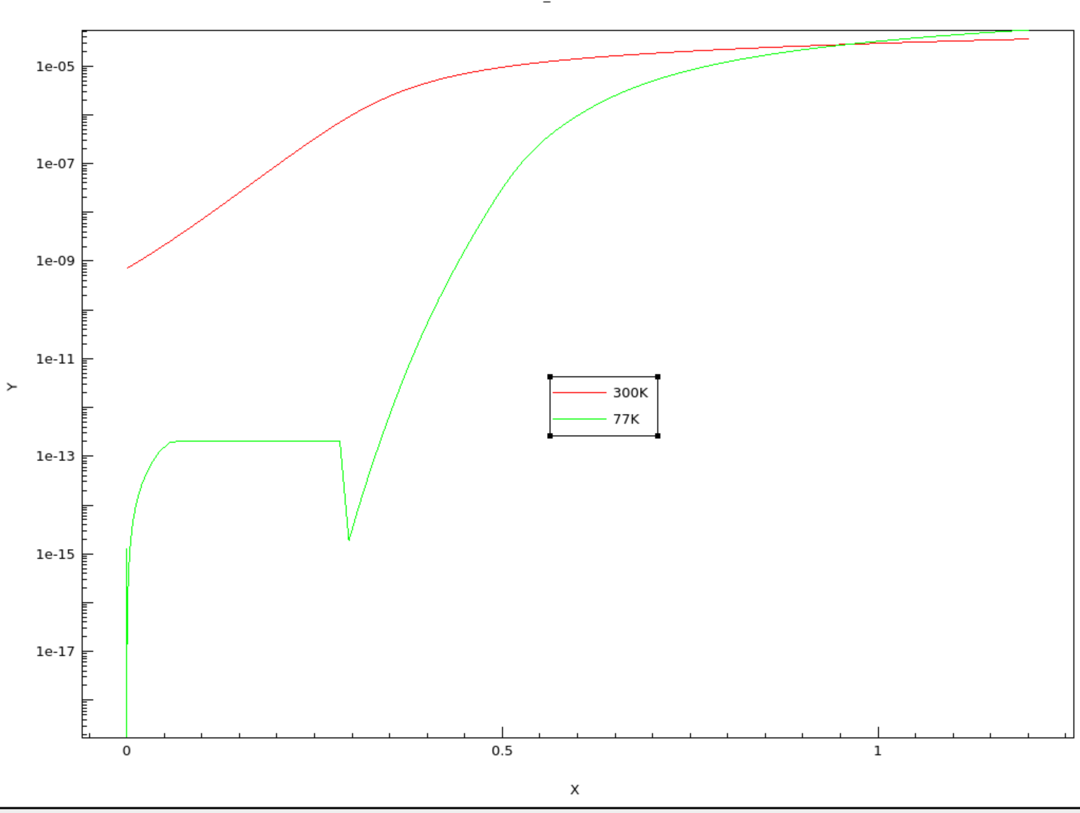
目前Vd=0.1V下的Vg-Id结果,环境温度在77K和300K下的结果。


 1232
1232

 被折叠的 条评论
为什么被折叠?
被折叠的 条评论
为什么被折叠?
 到【灌水乐园】发言


