


注:本文为 “FPGA 简介 / 工作原理” 相关文章合辑。
英文引文,机翻未校。
中文引文,未整理去重。
图片受引文原图所限不清晰。
How Does an FPGA Work?
Contributors: Alchitry, Ell C
Introduction
介绍
Let’s start at the beginning. What is an FPGA~? Well, FPGA stands for Field Programmable Gate Array, which isn’t helpful in understanding what they are or do but we had to get that out of the way.
让我们从头开始。什么是 FPGA?嗯,FPGA 代表现场可编程门阵列,这对理解它们是什么或做什么没有帮助,但我们必须把它弄清楚。
FPGAs belong to a class of devices known as programmable logic, or sometimes referred to as programmable hardware. Essentially, an FPGA doesn’t do anything itself but it can be configured to be just about any digital circuit you want. The magic here is that nothing physically changes. You simply load a configuration into the FPGA and it starts behaving like the circuit you wanted. No soldering, no jumper wires, no fuss. An FPGA can then be reconfigured to behave like another circuit, and another, and another. The configuration is RAM based which means it can essentially be reconfigured an unlimited number of times.
FPGA 属于一类称为可编程逻辑的设备,有时也称为可编程硬件。从本质上讲,FPGA 本身不做任何事情,但它可以配置为您想要的几乎任何数字电路。这里的神奇之处在于,物理上没有任何变化。您只需将配置加载到 FPGA 中,它就会开始像您想要的电路一样运行。无需焊接,无需跳线,无需大惊小怪。然后,可以重新配置 FPGA,使其行为像另一个电路,另一个电路,另一个电路。该配置是基于 RAM 的,这意味着它基本上可以无限次地重新配置。
Lattice iCE40 HX FPGA highlighted on the Alchitry Cu Board

Xilinx Artix 7 FPGA highlighted on the Alchitry Au Board

Even though we talk about using FPGAs to create digital circuits, you don’t typically draw schematics to create designs for them. The size and complexity of the circuits FPGAs can contain would become very cumbersome should you actually draw out a schematic. Instead, you can describe the behavior of the circuit you want and the tools will use this to create a circuit that matches that behavior.
尽管我们谈论的是使用 FPGA 来创建数字电路,但您通常不会绘制原理图来为它们创建设计。如果您实际绘制原理图,FPGA 可以包含的电路的大小和复杂性将变得非常繁琐。相反,您可以描述所需的电路行为,工具将使用它来创建与该行为匹配的电路。
In this regard it can feel like programming since you are just typing text. However, the fundamental implementation is drastically different as you are creating hardware.
在这方面,它可能感觉像编程,因为您只是在输入文本。但是,在创建硬件时,基本实现方式截然不同。
If creating hardware with text seems like magic, don’t worry. The way they work is actually quite simple in concept and in this tutorial we are going to really break it down.
如果使用文本创建硬件看起来很神奇,请不要担心。它们的工作方式实际上在概念上非常简单,在本教程中,我们将真正分解它。
Suggested Reading
推荐阅读
In this tutorial we are going to explore what an FPGA is and how they work. I’m going to assume you have a decent understanding of electricity (voltage, current, etc) and binary values. Everything else will be quickly built upon the basics. This is intended as an overview of what an FPGA is and its fundamental design, not a guide to designing your own.
在本教程中,我们将探讨什么是 FPGA 以及它们是如何工作的。我假设你对电力(电压、电流等)和二进制值有很好的理解。其他一切都将很快建立在基础之上。本文旨在概述什么是 FPGA 及其基本设计,而不是设计自己的指南。
If you aren’t familiar with the following concepts, we recommend checking out these tutorials before continuing.
如果您不熟悉以下概念,我们建议您先查看这些教程,然后再继续。
Voltage, Current, Resistance, and Ohm’s Law
电压、电流、电阻和欧姆定律
Learn about Ohm’s Law, one of the most fundamental equations in all electrical engineering.
了解欧姆定律,所有电气工程中最基本的方程之一。
What is Electricity?
什么是电?
We can see electricity in action on our computers, lighting our houses, as lightning strikes in thunderstorms, but what is it? This is not an easy question, but this tutorial will shed some light on it!
我们可以在电脑上看到电的作用,它照亮我们的房屋,闪电在雷雨中闪烁,但电是什么?这不是一个容易回答的问题,但本教程将为你提供一些启示!
Analog vs. Digital
模拟与数字
This tutorial covers the concept of analog and digital signals, as they relate to electronics.
本教程涵盖了与电子学相关的模拟信号和数字信号的概念。
Transistors
晶体管
A crash course in bi-polar junction transistors. Learn how transistors work and in which circuits we use them.
关于双极型晶体管的速成课程。学习晶体管的工作原理以及我们在哪些电路中使用它们。
Digital Circuits and Logic Gates
数字电路和逻辑门
Digital Circuits
数字电路
One caveat of FPGAs is that they can only create digital circuits. Some of the newer FPGAs include on-board analog to digital converters, but even these convert the analog input into a digital signal as soon as possible. But what is a digital circuit?
FPGA 的一个警告是,它们只能创建数字电路。一些较新的 FPGA 包括板载模数转换器,但即使是这些转换器也能尽快将模拟输入转换为数字信号。但什么是数字电路?
In electronics, digital is used to describe circuits that abstract away continuous voltage values in favor of discrete 1s and 0s. The actual voltages used and the thresholds don’t actually matter for the higher level design but you will often see something like 0V being a 0 and 1.2V being a 1 inside the FPGA. If the actual voltage is, say, 0.8V that is close enough to 1.2V to be considered a 1 and everything works the same.
在电子学中,数字用于描述抽象出连续电压值以支持离散 1 和 0 的电路。实际使用的电压和阈值对于更高级别的设计实际上并不重要,但您通常会在 FPGA 内部看到 0V 是 0,1.2V 是 1。例如,如果实际电压为 0.8V,则足够接近 1.2V,可以被视为 1,并且一切正常。
A digital circuit is designed to push the voltages to the extremes which makes them incredibly resilient to noise and other real-world interference. The concept of digital also gives us a way to design complicated behavior into the circuit without having to worry about the lower level design. We get to work in an ideal world. The nitty gritty is taken care of in the design of the simple building blocks that we will be using.
数字电路旨在将电压推至极值,这使得它们对噪声和其他现实世界干扰具有难以置信的抵抗力。数字化的概念还为我们提供了一种在电路中设计复杂行为的方法,而不必担心较低级别的设计。我们在一个理想的世界里工作。在我们将使用的简单构建块的设计中,细节得到了照顾。
These building blocks are logic gates.
这些构建块是逻辑门。
Logic Gates
逻辑门
There are a handful of different logic gates but the most common ones are AND, OR, XOR, and NOT. Each of these takes digital inputs, performs its logical function, and outputs a digital value.
有一些不同的逻辑门,但最常见的是 AND、OR、XOR 和 NOT。它们中的每一个都接受数字输入,执行其逻辑功能,并输出数字值。
An AND gate takes two inputs and outputs a 1 only when the first input and the second input are 1. If either input is 0, the output is 0. The symbol of an AND gate looks like this:
当第一个输入和第二个输入为 1 时,AND 门接受两个输入并输出 a 1。如果任一输入为 0,则输出为 0。AND 门的符号如下所示:

An OR gate takes two inputs and outputs a 1 when either the first input or the second input is 1. Only when both are 0 is the output 0. Here’s the OR gate symbol:
OR 门接受两个输入,当第一个输入或第二个输入为 1 时输出 1。只有当两者都为 0 时,输出才为 0。以下是 OR 门符号:

An XOR gate is similar to an OR gate but only outputs a 1 when either the first input or the second input are 1, but not when both are 1. It can also be thought of as outputting a 1 when the inputs are different. The X in XOR stands for exclusive. Here is its symbol:
XOR 门类似于 OR 门,但仅当第一个输入或第二个输入为 1 时输出 1,而当两者都为 1 时不输出 1。当输入不同时,也可以将其视为输出 1。XOR 中的 X 代表排他性。这是它的象征:

A [NOT](https://en.wikipedia.org/wiki/Inverter_(logic_gate )) gate is the simplest gate. It has one input and simply outputs the opposite of whatever it is. So a 1 becomes a 0 and a 0 becomes a 1.
非门是最简单的门。它有一个输入,并且只是输出与它是什么相反的输入。所以 1 变成 0,0 变成 1。

There are variations of the basic gates known as NAND, NOR, and XNOR. These are simply the standard versions with their outputs inverted.
基本门有多种变体,称为 NAND、NOR 和 XNOR。这些只是标准版本,其输出是反转的。
Just for some extra context, an AND gate, like all logic gates, can be built using transistors. The image below shows an example of how an AND gate could be implemented. The schematic uses NMOS and PMOS MOSFET transistors. This type of design is known as CMOS (complementary metal-oxide semiconductor) and is what is used in most modern circuits.
只是为了提供一些额外的背景信息,像所有逻辑门一样,AND 门可以使用晶体管来构建。下图显示了如何实现 AND 门的示例。原理图使用 NMOS 和 PMOS MOSFET 晶体管。这种类型的设计被称为 CMOS(互补金属氧化物半导体),是大多数现代电路中使用的设计。

Note that the above schematic is actually a NAND gate followed by a NOT gate. This is because CMOS circuits invert the output.
请注意,上述原理图实际上是一个 NAND 门,后面跟着一个 NOT 门。这是因为 CMOS 电路会反转输出。
Multiplexers
多路复用器
Now that we have the basic building blocks from transistors to logic gates, we can make something more useful with them. With just logic gates, you can describe any digital circuit. However, there are many reoccurring higher level functions that get their own symbols such as those used for binary math (adders, multipliers, etc).
现在我们已经有了从晶体管到逻辑门的基本构建模块,我们可以用它们制作出更有用的东西。仅使用逻辑门,即可描述任何数字电路。但是,有许多重复出现的高级函数获得自己的符号,例如用于二进制数学的符号(加法器、乘法器等)。
We are going to look at one of the fundamental building blocks of FPGAs, the multiplexer.
我们将研究 FPGA 的基本构建模块之一,即多路复用器。
A multiplexer selects a single input out of set based on the value of its select input. Here is its symbol:
多路复用器根据其选择输入的值选择设置外的单个输入。这是它的象征:

The /on the sel line is used to show it is 6 bits wide.
sel 行上的 / 用于表示它的宽度为 6 位。
The number of inputs will vary but the multiplexer always just has one output.
输入的数量会有所不同,但多路复用器始终只有一个输出。
The way the select input is encoded will also vary. Usually, you will see it as a binary number, but the simpler circuit uses a one-hot encoding. A one-hot encoding is simply a binary value where there is always exactly one 1. The position of the 1 is the important thing.
select 输入的编码方式也会有所不同。通常,您会将其视为二进制数,但更简单的电路使用独热编码。独热编码只是一个二进制值,其中总是只有一个 1。1 的位置很重要。
A decoder takes a binary value and turns it into a one-hot signal. An encoder turns a one-hot value into a binary number. These can be used to make a one-hot multiplexer accept binary values.
解码器接受二进制值并将其转换为一热信号。编码器将一个热值转换为二进制数。这些可用于使单热多路复用器接受二进制值。
Take a look at how we could implement a one-hot encoded multiplexer using just some AND and OR gates.
看看我们如何仅使用一些 AND 和 OR 门来实现一热编码多路复用器。

If we set the sel value to be 000010, meaning only sel [1] is 1, then we can see that for every AND gate, except for the one with the b input, one of the inputs will be 0. That means that each of those will always output 0 regardless of what the inputs a, c, d, e, and f are. The only input that matters is b. When b is 1, it is AND’d with a 1 and the output of the AND gate is 1. When b is 0, it is AND’d with 1 and the output of the AND gate is 0.
如果我们将 sel 值设置为 000010,这意味着只有 sel [1] 是 1,那么我们可以看到,对于每个 AND 门,除了具有 b 输入的门,其中一个输入将为 0。这意味着无论输入 a、c、d、e 和 f 是什么,它们中的每一个都将始终输出 0。唯一重要的输入是 b。当 b 为 1 时,它是 AND,其 1 为 AND,AND 门的输出为 1。当 b 为 0 时,它是 AND’d 与 1,AND 门的输出为 0。
In other words, the output of the AND gate is simply b.
换言之,AND 门的输出就是 b。

Result of the AND gates with sel [1] set to 1
The OR gate in this schematic is shown with more than two inputs. This can be created by creating a tree of two input OR gates where two inputs are OR’d together and the outputs are then OR’d together over and over until you have one output. A multi-input OR gate behaves just as you would expect with the output being 1 if any of the inputs are 1.
此原理图中的 OR 门显示有两个以上的输入。这可以通过创建两个输入 OR 门的树来创建,其中两个输入一起进行 OR 对接,然后输出一起进行 OR 对接,一遍又一遍,直到您有一个输出。多输入 OR 门的行为与您预期的一样,如果任何输入为 1,则输出为 1。
However, in this circuit every input to the OR gate is guaranteed to be 0 except the input from the AND gate whose output is b. This means that the OR gate will simply output a 1 when b is 1 and a 0 when b is 0.
但是,在该电路中,OR 门的每个输入都保证为 0,但 AND 门的输入除外,其输出为 b。这意味着当 b 为 1 时,OR 门将简单地输出 1,当 b 为 0 时,OR 门将简单地输出 0。
In other words, the output of the OR gate is simply b.
换言之,OR 门的输出就是 b。

Result of the OR gate will be b
You could repeat this logic for any input and, as long as the input is one-hot, the input that corresponds to the given 1 will be passed through to the output.
您可以对任何输入重复此逻辑,只要输入为 1-hot,对应于给定 1 的输入将被传递到输出。
You can imagine having a large matrix of multiplexers with a programmable sel input. This would allow you to route signals wherever you needed in your design. This is how FPGAs get their signals where they need to be and it is called the general routing matrix.
您可以想象有一个带有可编程 sel 输入的大型多路复用器矩阵。这将使您能够在设计中需要的任何位置路由信号。这就是 FPGA 如何将信号获取到需要的位置,它被称为通用路由矩阵。
Obviously the details for routing thousands and thousands of signals gets messy, but fundamentally it is just using a bunch of multiplexers with select inputs connected to programmable memory.
显然,路由成千上万个信号的细节变得混乱,但从根本上说,它只是使用一堆多路复用器,这些多路复用器的选择输入连接到可编程存储器。
Look-Up Tables
查找表
So now that we have a way to dynamically route signals wherever they need to be, we need a way to perform arbitrary logic. We will again be using multiplexers, or rather a descendant of them known as LUTs or look-up tables.
因此,既然我们有了一种方法可以动态地将信号路由到需要的任何地方,那么我们需要一种方法来执行任意逻辑。我们将再次使用多路复用器,或者更确切地说是它们的后代,称为 LUT 或查找表。
Imagine we have a multiplexer with four inputs and a 2 bit binary select (instead of one-hot). Now, instead of exposing the main inputs to the world, let’s hook them up to some programmable memory. This means we can program each input to some constant value. Wrap this all up into a block and we have a two input LUT.
想象一下,我们有一个多路复用器,具有四个输入和一个 2 位二进制选择(而不是一个热)。现在,让我们不要向世界公开主要输入,而是将它们连接到一些可编程内存。这意味着我们可以将每个输入编程为某个常数值。把这些都包成一个块,我们就得到一个两个输入的 LUT。

The two inputs to the LUT are the select inputs of the multiplexer. By programming the multiplexer inputs to be whatever we want, we can use this LUT to implement ANY two-to-one binary function.
LUT 的两个输入是多路复用器的选择输入。通过将多路复用器输入编程为我们想要的任何东西,我们可以使用此 LUT 来实现任何二对一二进制函数。
For example, we could make it act like a simple AND gate by setting the contents of the memory to be as follows.
例如,我们可以通过将内存内容设置为以下方式,使其像一个简单的 AND 门一样运行。
| Address (In [1:0]) | Value (Out) |
|---|---|
| 00 | 0 |
| 01 | 0 |
| 10 | 0 |
| 11 | 1 |
This is a simple example - normally LUTs are bigger than just two inputs and the FPGA on the Alchitry Au is based around five input LUTs.
这是一个简单的例子 - 通常 LUT 大于两个输入,而 Alchitry Au 上的 FPGA 基于五个输入 LUT。
Xilinx actually puts two five input LUTs together with another multiplexer to create either a six input LUT or a five input LUT with two independent outputs.
Xilinx 实际上将两个 5 输入 LUT 与另一个多路复用器放在一起,以创建 6 输入 LUT 或具有两个独立输出的 5 输入 LUT。

If you want to really dive into what the LUTs and resources in the FPGA look like, check out this document from Xilinx on the Artix 7. This document is very dense. You’ve been warned. Page 20 is worth a glance though. It shows a simplified schematic of a SLICEL. Slices are one building-block above LUTs. The four boxes on the left are the LUTs like shown above.
如果您想真正深入了解 FPGA 中的 LUT 和资源是什么样子的,请查看 Xilinx 关于 Artix 7 的这份文档。这个文件非常密集。你已经被警告过了。不过,第 20 页值得一看。它显示了 SLICEL 的简化原理图。切片是 LUT 之上的一个构建块。左边的四个框是 LUT,如上图所示。
For some context, the FPGA on the Alchitry Au has 20,800 dual LUTs. That’s a lot of LUTs but not even close to the largest FPGAs available which have about 260x that amount at the time of writing. As you can imagine, the routing of all those signals alone is insanely complex. Luckily for us, to use FPGAs you don’t need to do any of that. The tools take care of all the low level routing and LUT programming. We just get to describe the circuits we want.
在某些情况下,Alchitry Au 上的 FPGA 有 20,800 个双 LUT。这是很多 LUT,但甚至还不及可用的最大 FPGA,在撰写本文时,FPGA 的数量约为 260 倍。可以想象,仅所有这些信号的路由就非常复杂。幸运的是,要使用 FPGA,您不需要做任何这些事情。这些工具负责所有低级路由和 LUT 编程。我们只需要描述我们想要的电路。
Why Use an FPGA?
为什么要使用 FPGA?
Hopefully this tutorial has given you a warm fuzzy feeling for how FPGAs actually work, but why would you use one?
希望本教程能让您对 FPGA 的实际工作方式有一种温暖的模糊感觉,但您为什么要使用它呢?
Usually when this question comes up it’s in the context of choosing between using a processor or creating a custom design with an FPGA. Lots of people know how to code, far fewer understand how to create designs for FPGAs. Writing code is often easier to create complex behavior and to drastically change how something is implemented.
通常,当这个问题出现时,它是在使用处理器或使用 FPGA 创建定制设计之间进行选择的背景下进行的。很多人知道如何编码,但很少有人知道如何为 FPGA 创建设计。编写代码通常更容易创建复杂的行为,并彻底改变某些东西的实现方式。
However, FPGAs can be far more efficient in terms of processing time as well as offering very tight timing. To illustrate this, let’s look at a trivial example of turning an LED on when you press a button. If you wrote code to do this with something like an Arduino, the processor would run a small loop of code that would read the state of a pin then update the state of another pin based on that value.
然而,FPGA 在处理时间方面效率要高得多,并且时间紧迫。为了说明这一点,让我们看一个在按下按钮时打开 LED 的简单示例。如果您编写代码来使用 Arduino 之类的东西来执行此操作,处理器将运行一个小代码循环,该代码将读取一个引脚的状态,然后根据该值更新另一个引脚的状态。
If you optimized the code you could probably get this to update in the millions of times per second. That may sound great but let’s look at what it would look like with an FPGA. In the case of simply connecting a button to an LED with an FPGA, you simply connect the button and the LED. The value from the button passes through some input buffer, is fed through the routing matrix, then output through an output buffer. This process happens continuously all the time. The only delay comes from the switching delays of the transistors in the chip, which are incredibly small.
如果你优化了代码,你可能会让它以每秒数百万次的速度更新。这听起来可能很棒,但让我们看看使用 FPGA 会是什么样子。如果只需使用 FPGA 将按钮连接到 LED,则只需连接按钮和 LED。来自按钮的值通过某个输入缓冲区,通过路由矩阵馈送,然后通过输出缓冲区输出。这个过程一直在持续发生。唯一的延迟来自芯片中晶体管的开关延迟,这些晶体管非常小。
To expand on this, let’s now add a microphone to our design. We could take samples from the microphone and do some processing on it to figure out the frequencies in the captured audio. From some first hand experience, I know this is pretty hard to do on a small microcontroller in real time with any decent sampling rate. The processor needs to juggle reading in samples from the microphone, storing them in some buffer, performing a bunch of math, then output the values to maybe a display of LEDs. Each of these steps takes time and the processor can only really do one at a time.
为了扩展这一点,现在让我们在我们的设计中添加一个麦克风。我们可以从麦克风中取样,并对其进行一些处理,以找出捕获音频中的频率。根据一些第一手经验,我知道这在具有任何良好采样率的小型微控制器上实时完成是相当困难的。处理器需要处理从麦克风读取样本的问题,将它们存储在某个缓冲区中,执行一系列数学运算,然后将值输出到可能由 LED 组成的显示器上。这些步骤中的每一个都需要时间,而处理器一次只能真正完成一个。
With an FPGA, you could dedicate a small piece of your design to reading in samples from the microphone. This could then hand off the samples to a buffer, which, when full, would hand them off to a circuit that would do the calculations. That circuit could then hand off the results to another circuit that would display them on some LEDs.
借助 FPGA,您可以将设计的一小部分专门用于读取来自麦克风的样本。然后,可以将样本交给缓冲液,当缓冲液装满时,缓冲液会将它们交给进行计算的电路。然后,该电路可以将结果传递给另一个电路,该电路会将它们显示在一些 LED 上。
Each of these stages would operate entirely independently from one another since they simply exist in hardware. They aren’t lines of code competing for processor time.
这些阶段中的每一个都将完全独立地相互运行,因为它们只是存在于硬件中。它们不是争夺处理器时间的代码行。
Now imagine we still want the button hooked up to the LED. Our previous spectacular response time of a millionth of a second is now an abysmal fifth of a second because we can’t spare the processor time to read the button that often. However, in the FPGA the button and LED are still just connected together and responding at the near instantaneous speed as before.
现在想象一下,我们仍然希望将按钮连接到 LED。我们以前百万分之一秒的惊人响应时间现在是可怕的五分之一秒,因为我们无法让处理器有时间经常读取按钮。然而,在 FPGA 中,按钮和 LED 仍然只是连接在一起,并像以前一样以接近瞬时的速度响应。
This independence makes FPGAs a fantastic candidate for controlling anything that requires tight timing. For example, the WS2812B LED (aka NeoPixel) requires a tightly timed stream of pulses to write data to them. When you use a microcontroller, you usually need to write some inline-assembly just to get the timing of the pulses to be accurate enough. You also need to disable interrupts as any stalls would be detrimental to the signal.
这种独立性使 FPGA 成为控制任何需要严格时序的设备的绝佳候选者。例如,WS2812B LED(又名 NeoPixel)需要严格定时的脉冲流才能向其写入数据。当您使用微控制器时,通常需要编写一些内联程序集,以使脉冲的时间足够准确。您还需要禁用中断,因为任何停顿都会对信号造成不利影响。
With an FPGA, it is simple to create a series of tightly controlled pulses to drive these LEDs and you don’t need to worry about anything else in your design conflicting with the timing.
使用 FPGA,可以轻松创建一系列严格控制的脉冲来驱动这些 LED,而且您无需担心设计中的任何其他内容与时序冲突。
When to Use an FPGA
何时使用 FPGA
Given all the pros of using FPGAs, you may be asking yourself “Why wouldn’t I use one for everything!” Great question!
考虑到使用 FPGA 的所有优点,您可能会问自己 “为什么我不在所有事情上都使用一个呢!好问题!
In the description of how FPGAs work, you may have noticed that there’s a lot of extra “stuff” that has to go on to implement even the simplest circuit dynamically. This isn’t without its cost, and I mean that both in $$$ and in design resources.
在描述 FPGA 如何工作时,你可能注意到即使是实现最简单的电路,也需要进行大量额外的 “附加操作”。这并不是没有代价的,我的意思是无论是在成本上还是在设计资源上。
FPGAs tend to be expensive. The larger ones easily go for tens of thousands of dollars PER CHIP. This is due to the amount of silicon required to make them, the huge amount of RnD to design the chips and the tools, and the relatively low volume compared to things like tiny processors used in phones.
FPGA 往往很昂贵。较大的芯片很容易达到每个芯片数万美元。这是由于制造它们所需的硅量,设计芯片和工具所需的大量 RnD,以及与手机中使用的微型处理器等设备相比,体积相对较小。
Another cost is power. There are a lot of transistors used in the LUTs compared to the number needed to implement the circuit directly. All these transistors require power to operate. Because of this, FPGAs tend to be poor candidates for battery operated devices. You can of course design your circuits to be power efficient but even doing absolutely nothing, the FPGA on the Alchitry Au consumes a little over 100mA. You can easily get over 1000mA if you start pushing the chip. As a comparison the ATmega32U4, the chip used on the Arduino Leonardo, uses 27mA when running with 5V at full speed. Granted the Alchitry Au is substantially more capable.
另一个成本是电力。与直接实现电路所需的数量相比,LUT 中使用了很多晶体管。所有这些晶体管都需要电源才能运行。正因为如此,FPGA 往往不适合电池供电的设备。当然,您可以将电路设计为节能高效,但即使什么都不做,Alchitry Au 上的 FPGA 消耗的电流也会略高于 100mA。如果你开始推动芯片,你可以很容易地获得超过 1000mA 的电流。相比之下,Arduino Leonardo 上使用的芯片 ATmega32U4 在全速运行 27V 时使用 5mA。当然,Alchitry Au 的能力要强得多。
So why use FPGAs at all? Well, you have two major alternatives to creating a custom digital circuit. First, you could build it yourself out of discrete logic. This would take a significant amount of time, likely cost significantly more, and have little flexibility if you needed to change something.
那么,为什么要使用 FPGA 呢?那么,您有两种主要的替代方法来创建自定义数字电路。首先,你可以自己用离散逻辑来构建它。这将花费大量时间,可能会花费更多,并且如果您需要更改某些内容,则几乎没有灵活性。
The second, and more realistic, alternative is to create the circuit directly in silicon. This creates a very fast, very efficient circuit, but at the cost of zero flexibility and truck loads of $$$. Custom silicon has huge upfront costs associated with the tooling and setup. The incremental cost per chip would be lower than individual FPGAs though. However, unless you’re making tens of thousands of chips, this will be more expensive overall. Even then, it sometimes doesn’t make sense to lock your design into silicon. With an FPGA you can change it whenever you need to without penalty.
第二种更现实的选择是直接在硅上创建电路。这种方法可以创造出非常快速、效率极高的电路,但代价是完全没有灵活性,并且需要大量的资金。定制硅的工具和设置具有巨大的前期成本。然而,每个芯片的增量成本通常低于单独的 FPGA。不过,除非你打算生产数万个芯片,否则总体成本会更高。即便如此,有时候将设计锁定在硅上也并不明智。使用 FPGA,你可以在需要时随时进行更改,而不会产生额外的费用。
Because of their flexibility and low-cost compared to the alternatives, FPGAs open the doors to adding custom digital circuits to just about any design. But, do you really need a custom circuit?
由于与替代产品相比,FPGA 具有灵活性和低成本,因此为向几乎任何设计添加定制数字电路打开了大门。但是,您真的需要定制电路吗?
It is important to keep in mind that FPGAs are just like any other tool. A hammer is great for nailing in nails, but it is terrible for screwing in screws. Just as trying to nail a nail with a screwdriver would be quite futile.
重要的是要记住,FPGA 就像任何其他工具一样。锤子非常适合钉入钉子,但拧入螺丝则很糟糕。就像试图用螺丝刀钉钉子一样,这将是徒劳的。
Creating custom circuits can be difficult and you often need to ask yourself if there is a better solution. There are many very capable processors with tons of peripherals that can handle most of the problems you need to solve. Trying to do something like sending and receiving data over WiFi would be a daunting task with an FPGA but is easily accomplished with a few dollar microcontroller like the ESP8266.
创建定制电路可能很困难,您经常需要问问自己是否有更好的解决方案。有许多非常有能力的处理器和大量的外围设备可以处理您需要解决的大部分问题。尝试通过 WiFi 发送和接收数据之类的事情对于 FPGA 来说将是一项艰巨的任务,但使用像 ESP8266 这样的几美元的微控制器可以轻松完成。
I often describe FPGAs as an assembly line. Each station on an assembly line works independent from each other and they are incredibly efficient at what they are designed for. However, it can be difficult to initially set up the line and if you want to make major changes it is often easier to start from scratch.
我经常将 FPGA 描述为一条装配线。装配线上的每个工位彼此独立工作,它们在设计目的上非常高效。但是,最初设置生产线可能很困难,如果您想进行重大更改,从头开始通常更容易。
On the other hand, processors are like people. A single person could do just about any task given enough time and the training. Complex sequential tasks are easy for a person to accomplish.
另一方面,处理器就像人一样。只要有足够的时间和培训,一个人就可以完成几乎任何任务。复杂的顺序任务对一个人来说很容易完成。
Do you really want to set up an entire sandwich manufacturing plant just to make you a sandwich for lunch?
你真的想建立一个完整的三明治制造厂,只是为了让你做午餐的三明治吗?
FPGAs are amazing and often indispensable for the tasks they excel at but they are just another tool to add to your toolbox. A very powerful and worthwhile tool to invest in, but still just another tool.
FPGA 非常出色,对于它们擅长的任务来说通常是不可或缺的,但它们只是添加到您工具箱中的另一种工具。一个非常强大且值得投资的工具,但仍然只是另一种工具。
FPGA基础知识----FPGA 简介
原来如此呀于 2021-10-26 20:20:57 发布
FPGA 简介
第1节 什么是 FPGA
FPGA 的全称为 Field-Programmable Gate Array,即现场可编程门阵列。 FPGA 是在 PAL、 GAL、 CPLD 等可编程器件的基础上进一步发展的产物, 是作为专用集成电路( ASIC)领域中的一种半定制电路而出现的,既解决了定制电路的不足,又克服了原有可编程器件门电路数有限的缺点。 简而言之, FPGA 就是一个可以通过编程来改变内部结构的芯片。
FPGA 功能实现:需要通过编程即设计硬件描述语言,经过 EDA 工具编译、综合、布局布线成后转换为可烧录的文件,
最终加载到 FPGA 器件中去,改变 FPGA 内部的连线,最终完成所实现的功能。
FPGA 性能对比:FPGA 相比于单片机、 CPU 等集成电路芯片拥有效率更高、功耗更低的特点,但是易于开发程度远远不如单片机、 CPU; 在数字芯片设计领域, FPGA 虽然相比 ASIC 具有更短的开发周期与开发难度, 但是其存在着成本过高、性能较差并且在资源的利用率上远不及 ASIC 等问题,不能真正的替代 ASIC。
第2节 FPGA 的基本结构
FPGA 可编程的特性决定了其实现数字逻辑的结构不能像专用 ASIC 那样通过固定的逻辑门电路来完成,而只能采用一种可以重复配置的结构来实现, 而查找表(LUT)可以很好地满足这一要求,目前主流的 FPGA 芯片仍是基于 SRAM 工艺的查找表结构。
FPGA 芯片参数指标:包含可编程逻辑模块的数量、固定功能逻辑模块(如乘法器)的数目及存储器资源(如嵌入式 RAM)的大小。
在最底层的可配置逻辑模块(如片上的逻辑单元) 上,存在着基本的两种部件:触发器和查找表( LUT) , 而触发器和查找表的组合方式不同,是各个 FPGA 家族之间区别的重要依据, 并且查找表本身的结构也可能各不相同( 有 4 输入或 6 输入或其他)。
查找表( Look-Up-Table)简称为 LUT, 其本质上就是一个 RAM。目前 FPGA 内部中多使用 4输入的 LUT,每一个 LUT 可以看成一个有 4 位地址线的 RAM。
当用户在 EDA 工具上通过原理图或 硬件描述语言设计了一个逻辑电路以后, FPGA 开发软件会自动计算逻辑电路的所有可能结果,并把真值表(即结果)事先写入 RAM 中。 这样,每输入一个信号进行逻辑运算就等于输入一个地址进行查找表操作, 通过地址找到对应的 RAM 中的结果, 最后将其输出。以实现数字逻辑 Y=A&B&C 的功能为例。如果是在专用 ASIC 中,为了实现该逻辑,逻辑门都已经事先确定好, Y 的输出值为两个逻辑与运算后的结果,其基本的实现结构如下图所示:

对Y=A&B&C 的 利用FPGA 实现基本结构 :

第3节 更为复杂的 FPGA 架构
随着技术的发展和工艺节点的进步, FPGA 的容量和性能在不断提高的同时, 其功耗却不断的优化减少。 2006 年以前四输入查找表一直被广泛使用, 在一些高端器件可能会用上六输入、八输入或更多输入端口的查找表。 而一个多输入的查找表又可以分解成较小输入的查找表, 即能够分裂成许多更小的功能。 例如一个八输入的查找表可以分解成两个四输入的查找表或分解成一个三输入加一个五输入的查找表。在实际的高端器件中,这种可编程构造可以描述相当于百万级(有时甚至千万级)的原始逻辑门。
在 FPGA 内部,利用 FPGA 的可编程性在芯片内部构造实现了一个计数器逻辑,有着“软内核”与“硬内核”之分。
软内核(软功能):在构造计数器逻辑过程中使用到的功能便可以被称为软功能。
硬内核(硬功能):功能若是直接用芯片实现的,则是利用了芯片内部的硬功能。
软内核与硬内核之间优势互补,软内核的优势**在于可以在利用芯片资源的基础上**利用编程设计让其完成需要实现的任何功能(注意是数字功能,不包括模拟功能)。 而硬内核由于是实现固定功能的器件,因此其优势在于资源利用率高且功耗较低, 占用硅片的面积也较小, 并具有较高的性能。最重要的区别在于:与软内核相比硬内核可用于实现模拟功能, 例如锁相环的倍频功能,这个功能需要在模拟电路下实现,所以这一部分是在 FPGA 内部用硬件来实现的 。
第4节 带嵌入式处理器的 FPGA
利用 FPGA 的可编程构造实现的事情之一即为使用其中的一部分数字逻辑资源制作一个或多个软处理器内核, 当然, 也可以实现不同规模的处理器。

这个芯片是一种新的SoC(System on Chip,系统级芯片) FPGA,完全以硬内核方式实现的双路 ARM Cortex-A9 微控制器子系统(运行时钟高达 1GHz,包含浮点引擎,片上缓存,计数器,定时器等)以及种类广泛的硬内核接口功能( SPI, I2C, CAN等),还有一个硬内核的动态内存控制器,所有这些组件都利用大量传统的可编程构造和大量的通用输入输出( GPIO)引脚进行了性能增强。
第5节 数据存储以及配置方式
在 FPGA 内部存在着存储单元片内 RAM 块,数据是存放在 RAM 中并由其来设置工作状态的,若想要 FPGA 进行工作,就需要对片内 RAM 进行编程。 而如果外部有大量数据交互时,就要通过增加外设来对数据进行暂时性的存储,如 SDRAM 存储器或者 DDR3 存储器,暂存在外设中的数据最终也是要通过 FPGA 内部的 RAM 进行存储与处理。当在 EDA 工具上将程序设计完成之后,便需要将软件上的程序烧录进 FPGA 内部。通过不同的配置模式, FPGA 便会有不同的编程方式。
常用的几种配置模式:
- 并行模式: 通过并行 PROM(Programmable read-only memory,可编程只读存储器)、 Flash (Macromedia Flash。多媒体软件平台)配置 FPGA;
- 主从模式: 使用一片 PROM 配置多片 FPGA;
- 串行模式:串行 PROM 配置 FPGA;
- 外设模式:将 FPGA 作为微处理器的外设,由微处理器对其编程。
目前, 主流的 FPGA 都是基于 SRAM (Static Random-Access Memory,静态随机存取存储器)工艺的, 在大部分的 FPGA 开发板上,使用的都是串行配置模式。由于 SRAM 掉电就会丢失内部数据,因此往往都会外接一个能够掉电保存数据的片外存储器以保存程序。 这样一来, 上电时 FPGA 便将外部存储器中的数据读入片内 RAM 以完成配置, 对 FPGA 编程完成后便进入工作状态;掉电后 FPGA 内部 SRAM 中存储的数据丢失,逻辑清零。 以这种方式配置 FPGA 不仅能反复使用,还无需重复的手动配置。完成一次主动配置之后每次上电便会自动的实现 FPGA 的内部编程。
FPGA 基础知识介绍
FPGA(Field-Programmable Gate Array),即现场可编程门阵列,它是在 PAL、GAL、CPLD 等可编程器件的基础上进一步发展的产物。它是作为专用集成电路(ASIC)领域中的一种半定制电路而出现的,既解决了定制电路的不足,又克服了原有可编程器件门电路数有限的缺点。
目前 FPGA 的两大主要厂商为 xilinx 和 altera。
Xilinx:公司网址为:www.xilinx.com。FPGA 市场的龙头老大,市场份额接近 50%,其主要产品包括:Sparten 系列、Virtex 系列、Artix 系列、Kintex 系列、Virtex 系列等
开发工具:其第六代及以前的产品的开发工具为 ISE,从第七代产品开始,已全部转移到 vivado 平台。
Altera:公司网址为:www.altera.com。FPGA 市场的二当家,市场份额 40% 以上,2015 年 6 月被 Intel 以 167 亿美元收购。主要产品包含:Max 系列、Cyclone 系列、Arria 系列、Stratix 系列等。主要开发工具:Quartus
此外,Lattice、Actel、Atmel 等公司也有 FPGA 产品,由于市场份额小,市面上很少见到,此处不再介绍。
FPGA 产品种类多种多样,但原理都是相同的。我们只要理解了其基本结构,学习起来还是非常轻松的。
在介绍 FPGA 之前,先对数字电路中所学的知识做一个简单的回顾。
现如今的集成电路绝大部分采用 CMOS 工艺,CMOS 电路是互补型金属氧化物半导体电路 (Complementary Metal-Oxide-Semiconductor) 的英文字头缩写,它由绝缘场效应晶体管组成,由于只有一种载流子,因而是一种单极型晶体管集成电路,其基本结构是一个 N 沟道 MOS 管和一个 P 沟道 MOS 管。NMOS 和 PMOS 可以认为是两种开关电路,两种电路均包含 G(栅极)、D(漏极)、S(源极)三个极:
对于 NMOS,当 G 为高电平时,D、S 导通,否则截止
对于 PMOS,当 G 为低电平时,D、S 导通,否则截止

一个 NMOS 和一个 PMOS 可构成一个 CMOS 反相器:
vi 为高电平时,PMOS 截止,NMOS 导通,vo 输出低电平
vi 为低电平时,PMOS 导通,NMOS 截止,vo 输出高电平

其逻辑表达式可写成:

同理,可构成 CMOS 的与非门、或非门

通过非门、与非门、或非门可实现所有的组合逻辑电路,多个与非门可组成一个带有复位、置位功能的 D 触发器,而 D 触发器则是时序逻辑电路的最核心部件。

由此可知,通过非门、与非门、或非门的有序堆叠,可实现任意功能的数字电路,如果有一款电路,其基本单元可配置成各种基本门,则其就具备了硬件编程能力。FPGA 就是这种芯片,它基于查找表(LUT:Look Up Table)技术的可编程逻辑器件,通过配置,LUT 可实现与门、或门、与非门、或非门或者其他简单组合逻辑功能,其本质上就是 1bit 位宽的 RAM
我们以一个 2 输入的查找表为例,来做讲解

以目前比较流行的 Spartan6 芯片为例,来说明
其最底层便是一个 6 输入查找表(可拆成两个 5 输入 LUT 使用)以及两个 D 触发器的结构

Slice 是 Xilinx FPGA 的最基本单元,包含 4 个 6 输入 LUT 及 8 个 D 触发器
Xilinx 的 FPGA 中包含三类 Slice:SliceL、SliceM、SliceX,三类 slice 本质上是相同的,只不过在细节上有一些差别,此处不再详细展开。

CLB(Configurable Logic Blocks)是 Sparten6 的主要资源,包含两个 Slice,如下图所示:

多个 CLB 再加上丰富的互联开关,便构成了 Xilinx 公司 FPGA 的最核心框架。
下图是 xilinx 一款型号为 XC6SLC45T 的 FPGA 在 planAhead 中的视图

从图中可以看出,FPGA 内部,除了大量的 CLB 资源,用于实现可编程逻辑外,还有一些其它的硬件资源,包括 block ram、内存控制器、时钟管理(CMT)单元、数字信号处理(DSP)端口控制(IOB)单元等,大大提高了其可编程性,几乎可以实现所有的数字电路功能。
下面是在 planahead 中对 xc6slx4-2tqg144 芯片的截图,通过这些图片,可以对其结构有一个整体的了解。更多的细节性问题,需要大家在实际使用过程中逐步掌握。

输入输出块,包含了焊盘及其相关电路

ILOGIC、OLOGIC、IODELAY 部分

Slice

Slice

Block RAM 资源

时钟管理单元

时钟驱动电路

FPGA 依靠其强大、全方面、多维度的可编程能力,在航空航天、电子通信、银行金融、医疗设备、信息存储、数据处理、ASIC 原型验证等许多行业或领域发挥着极其重要的作用。…
FPGA 的基本结构
拉钩上吊一百年于 2020-09-04 10:45:40 发布
一、总体结构

二、基本组成部分
1、可配置逻辑单元(Configurable Logic Block,CLB)
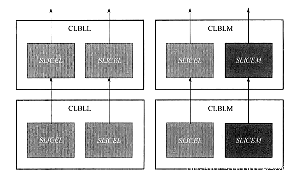
CLB 由两个 SLICE 构成,SLICE 可分为 SLICEL (L:Logic)和 SLICEM (M:Memory),因此 CLB 也可分为 CLBLL 和 CLBLM 两类。
SLICE 由查找表(LUT)和寄存器(Register) 组成,查找表完成纯组合逻辑功能。FPGA 内部寄存器可配置为带同步 / 异步复位和置位、时钟使能的触发器,也可以配置成为锁存器。FPGA 一般依赖寄存器完成同步时序逻辑设计。
学习底层配置单元的 LUT 和 Register 比率的重要意义在于器件选型和规模估算。
注意:FPGA 中组合逻辑全部使用查找表 LUT 实现,此外,查找表也可用来作为分布式存储使用。
2、可编程输入输出单元(IOB)
目前大多数 FPGA 的 I/O 单元被设计为可编程模式,即通过软件的灵活配置,可适应不同的电器标准与 I/O 物理特性;可以调整匹配阻抗特性,上下拉电阻;可以调整输出驱动电流的大小等。
3、嵌入式块 RAM
目前大多数 FPGA 都有内嵌的块 RAM。嵌入式块 RAM 可以配置为单端口 RAM、双端口 RAM、伪双端口 RAM、CAM、FIFO 等存储结构。
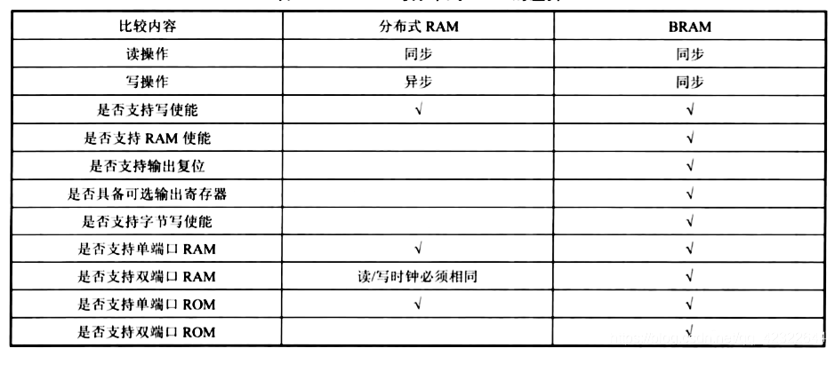
尽管 BRAM 的功能更多,但是对于一些小规模的数据存储,分布式 RAM 可能获得比 BRAM 更好的性能(从功耗和速度两方面讲)。
4、内嵌的底层功能单元和嵌入式专用硬核
底层嵌入功能单元是指通用程度较高的嵌入式功能模块。如锁相环 (Phase Locked Loop,PLL)、DLL (Delay Locked Loop)、DSP (Digital Signal Processing) 和 CPU 等。
与 “底层嵌入单元” 是有区别的,这里指的硬核主要是那些通用性相对较弱,不是所有 FPGA 器件都包含硬核。
5、完整的时钟管理
全局时钟是一种专用互联网络,是专为覆盖对 FPGA 中各种资源的所有时钟输入设计的。这些时钟网络的设计旨在降低歪斜、占空比失真和功耗。其设计的目的还在于支持甚高频信号。
全局时钟控制资源和网络通常由以下通路和组件构成:全局时钟输入 、全局时钟缓冲器 、时钟树和时钟网络 - GCLK 、时钟区域。
6、丰富的布线资源
长线资源、短线资源及逻辑单元內部布线资源。
FPGA工作原理、架构及底层资源
m0_74823595 2024-12-04 22:31:43
前言
随着数字电路设计和嵌入式系统应用的不断发展,FPGA(Field-Programmable Gate Array)作为一种灵活、可重构的可编程逻辑器件,受到了越来越广泛的关注和应用。本篇博客将探讨 FPGA 的原理、架构及底层资源,旨在为读者深入了解 FPGA 提供全面的专业知识。
一、FPGA 工作原理
FPGA 的原理基于可编程逻辑块和可编程互连网络。逻辑块是 FPGA 的基本组成单元,通常由查找表(Look-up Table,LUT)和寄存器组成。查找表是 FPGA 的关键组件之一,它是一种存储逻辑功能的表格结构,可以实现 2 输入至 6 输入的逻辑运算。随着技术的发展和 FPGA 的进化,FPGA 芯片中的逻辑块和查找表的规模不断增加,以满足更复杂的逻辑功能和应用需求。较高输入数量的查找表能够支持更多复杂的逻辑运算,提供更大的灵活性和性能优化。通过编程或配置查找表的值,可以改变逻辑功能的实现。寄存器用于存储状态或临时计算结果,在时钟信号的控制下进行数据的存储和传输。
FPGA 的可编程互连网络负责将逻辑块连接在一起以形成所需的电路拓扑。它由全局连线和局部连线两部分组成。全局连线是一组专用的高速互联通道,用于实现逻辑块之间的远距离连接,例如跨时钟域的连接。局部连线则是邻近的逻辑块之间的连线,用于实现邻近互连关系。FPGA 的互连网络可通过编程开关(Programmable Switch)的控制以实现连线的通断,使得逻辑块之间的连接变得灵活可变。
深入理解:如果把 FPGA 理解为一块电路板,设计师则是利用这块电路板,通过选用器件和选通布线的方式设计所需的电路。该板上有许多器件,且各类器件的位置已经固定,器件之间存在丰富的布线资源,器件和布线都可通过编程决定是否选用。设计过程就是根据功能选用不同的器件,再选通设计中的布线,最终形成目标电路。
二、FPGA 架构及底层资源
1. FPGA 架构

目前主流的 FPGA 仍以查找表技术为基础,主要由六部分组成:可编程输入输出单元(IOB)、可编程逻辑单元(CLB)、完整的时钟管理(DCM)、嵌入块状 RAM(BRAM)、布线资源、内嵌的底层功能单元(soft core,软核,区别于软 IP 核)和内嵌专用硬件模块(hard core,硬核,区别于硬 IP 核)。其中最为主要的是可编程输入输出单元、可编程逻辑单元和布线资源。
IP 核一般分为软 IP 核、硬 IP 核和固 IP 核,与上述的软硬核并不是同一个定义范畴。软核(soft core)和硬核(hard core)是 FPGA 中两种不同类型的处理器核心或其他复杂数字逻辑功能的实现方式。
软核(soft core)通常是指通过 FPGA 中的逻辑资源进行编程实现的处理器核心或其他复杂数字逻辑功能,它们的实现是通过 FPGA 内部的逻辑单元和存储单元来完成的。一个常见的软核是 Xilinx(现被 AMD 收购)的 MicroBlaze,它是一款可在 Xilinx FPGA 中实现的 32 位 RISC 处理器核心,设计者可根据自己的需求对其进行配置和定制,以满足特定的应用需求。另一个常见的软核是 Altera(现被 Intel 收购)的 Nios II,也是一款可在 FPGA 中实现的可编程处理器核心。
硬核(hard core)则是指在 FPGA 芯片的物理结构中以硬件形式实现的处理器核心或其他专用的硬件模块。这种硬件功能通常由 FPGA 芯片的制造厂商直接设计和实现,并在 FPGA 芯片中进行硬件布局,与 FPGA 中的逻辑资源分离。例如,一些 FPGA 芯片可能内置了 ARM 处理器的硬核,这些 ARM 处理器核心是作为 FPGA 芯片的一部分直接集成在硅片中,用户可直接利用这些处理器核心来实现特定的处理器功能,而不需要通过 FPGA 的逻辑资源来实现。
因此,软核和硬核代表了 FPGA 中实现处理器核心或其他复杂逻辑功能的两种不同方式。软核通过 FPGA 中的逻辑资源进行编程实现,而硬核则是直接作为 FPGA 硅片的一部分实现的,两者各有优劣,选择取决于具体的应用需求和设计考虑。
2. FPGA 底层资源
2.1 可编程输入/输出单元(IOB)
可编程输入/输出单元简称 I/O 单元,是芯片与外界电路的接口部分,用于完成不同电气特性下对输入/输出信号的驱动与匹配要求,其示意结构如图 1-2 所示。FPGA 内的 I/O 按组分类,每组都能够独立地支持不同的 I/O 标准。通过软件的灵活配置,可适配不同的电气标准与 I/O 物理特性,可以调整驱动电流的大小,可以改变上下拉电阻。目前,I/O 口的频率越来越高,一些高端的 FPGA 通过 DDR 寄存器技术可以支持高达多个 Gb/s 的数据速率。
外部输入信号可以通过 IOB 模块的存储单元输入到 FPGA 的内部,也可以直接输入 FPGA 内部。当外部输入信号经过 IOB 模块的存储单元输入到 FPGA 内部时,其保持时间(Hold Time)的要求可以降低,通常默认为 0。
为了便于管理和适应多种电气标准,FPGA 的 IOB 被划分为若干个组(bank),每个 bank 的接口标准由其接口电压 Vcco 决定,一个 bank 只能有一种 Vcco,但不同 bank 的 Vcco 可以不同。只有相同电气标准的端口才能连接在一起,Vcco 相同是接口标准的基本条件。

关于 IOB 需要注意:
IOB 的结构如上,PAD 即与外界连接焊盘引脚,同时有一个 IBUF 和 OBUF。当配置为 output 时,连接左边的 OBUF;配置为 input 时,连接右边的 IBUF。在 FPGA 中,每一个 IOB 都有与之对应的一个 xIOI3 模块(有 LIOI3 和 RIOI3 之分,由三个触发器 Flip-Flop 组成,TFF、OFF 和 IFF),且其布线资源比较固定,使用 xIOI3 中的触发器有一个较大的好处,就是其布线资源固定,且最靠近各个引脚,可以实现较低的延迟,在某些特定的场合如高速数据采样下,使用 xIOI3 可以实现良好的采样效果。如果不使用 IOB 的触发器而连接普通的 Slice 内部寄存器,则信号进入第一级寄存器的布线会因为每次综合结果的不同而各有不同,且由于 Slice 距离接口较远,有可能导致高速信号的采样不正确,不满足时序要求。
一般情况下 IOB 的寄存器缺省为 OFF,如果需要设置接口的寄存器,可以通过下列约束实现:
set_property IOB TRUE {get_ports your_port_name}
如果需要取消接口的寄存器,可以通过下列约束实现:
set_property IOB FALSE {get_ports your_port_name}
2.2 可配置逻辑块
可配置逻辑块 CLB(Configure Logic Block)是实现组合逻辑和时序逻辑的主要资源,由一对 Slice(片单元)组成,每一个 CLB 都连接到一个交换矩阵(Switch Matrix)中。
每个 Slice 资源包含 4 个 6 输入的 LUT,8 个 FF 以及 MUX 和 Carry。Slice 又可分为 SliceL 和 SliceM 两种类型,在 7 系列器件中,大约 2/3 的 Slice 为 SliceL,其余为 SliceM,两者的区别是 SliceM 可配置为分布式 RAM(Distribute RAM)和移位寄存器,SliceL 则不行。
每个 CLB 都包含一对 Slice,这对 Slice 可能都是 SliceL 或是一个 SliceL 和一个 SliceM。属于一个 CLB 中的 SliceL 和 SliceM 是独立的,无相互连接的线路,只有属于同一列的 Slice 之间才会通过进位链进行连接。每个 Slice 有一个坐标 XcYr,r 为 slice 的列序号,c 为行序号,同一个 CLB 的 slice 行序号是相同的。


2.3 丰富的布线资源
FPGA 芯片内部有丰富的布线资源,根据工艺、长度、宽度和分布位置的不同而划分为 4 类:
- 全局布线资源,用于芯片内部全局时钟和全局复位/置位的布线;
- 长线资源,用于完成芯片 bank 间的高速信号和第二全局时钟信号的布线;
- 短线资源,用于完成基本逻辑单元之间的逻辑互连和布线;
- 分布式的布线资源,用于专有时钟、复位等控制信号线。
在实际中,设计者不需要直接选择布线资源,布局布线器可自动地根据输入逻辑网表的拓扑结构和约束条件选择布线资源来连通各个模块单元。几乎遇不到需要手动去布局布线的情况。
2.4 数字时钟管理模块(DCM)
用于生成和管理芯片内部的时钟信号,包括时钟分频、相位锁定和时钟多路复用等功能,确保设计中的时序要求得到满足。目前,业内大多数 FPGA 均提供数字时钟管理,在内部资源中通常整合为 CMT(Clock Manage Tile,时钟管理模块),每个区域对应一个 CMT,一个 CMT 由一个 MMCM(Mix-mode Clock Manager)和 1 个 PLL(Phase Locked Loop)组成。主要起到频率综合、去抖动和去偏斜的作用。
对于我们一般设计者来说,最常见的就是用 DCM 去产生 FPGA 设计中要用到的时钟。
2.5 嵌入式块 RAM(BRAM)
-
架构和特性:
BRAM 是专门为 FPGA 设计而优化的存储资源。它是内置在 FPGA 中的硬件块,能够提供高速、低功耗和可配置的存储功能。BRAM 通常由多个存储块组成,每个存储块都有一个比特宽度和一个数据深度。每个存储块由一个寄存器数组、读取端口和写入端口组成。BRAM 可以被配置成单端口 RAM、双端口 RAM、内容寻址存储器(CAM)和 FIFO 等不同的存储结构,以适应各种应用需求。
-
容量和配置:
BRAM 的容量通常以位宽和深度来描述,例如 18Kbit 表示容量为 18 千比特,深度为 1024,常见的容量包括 18Kbit、36Kbit 等,不同型号的 FPGA 器件会提供不同大小和规格的 BRAM。BRAM 的位宽决定了每个存储位置可以存储的二进制位数,而深度则确定了存储位置的数量。开发者可以根据需要调整 BRAM 的位宽和深度来满足存储需求。
-
用途和应用:
BRAM 在 FPGA 中有广泛的应用场景。它可以用于存储程序指令、缓存数据、实现状态机或 FIFO 缓冲区等。BRAM 还可用于存储查找表(LUT)和存储器初始化值。对于存储器初始化值,可以在设计中使用 BRAM 以提高初始化数据的可读性和灵活性。
-
优势和注意事项:
BRAM 提供了低延迟和高带宽的存储能力,在许多应用中比分布式 RAM 更适合。使用 BRAM 可以节省逻辑资源,因为 BRAM 在 FPGA 中是内置的,不占用额外的逻辑单元。需要注意的是,使用 BRAM 需要合理规划存储容量,并注意时钟和数据控制信号的正确配置,以确保正确的数据存储和访问。
2.6 底层内嵌功能单元(soft core,软核,区别于软 IP 核)
内嵌功能模块主要指 DLL(Delay Locked Loop)、PLL(Phase Locked Loop)、DSP 和 CPU 等软处理核(Embeded Processor)。正是由于集成了丰富的内嵌功能单元,从而使得单片 FPGA 成为系统级的设计工具,具备了软、硬件联合设计的能力,逐步向 SoC 平台过渡。
DLL 和 PLL 具有类似的功能,可以完成时钟高精度、低抖动的倍频和分频,以及占空比调整和移相等功能。Xilinx 公司生产的芯片上集成了 DLL,Altera 公司的芯片集成了 PLL,Lattice 公司的新型芯片上同时集成了 PLL 和 DLL。PLL 和 DLL 可以通过 IP 核生成的工具方便地进行管理和配置。
2.7 内嵌专用硬核(hard core,硬核,区别于硬 IP 核)
FPGA 中的内嵌专用硬核是指在 FPGA 芯片中内置的、专门设计用来执行特定功能的硬件模块。这些专用硬核旨在提供特定的功能和性能,与可编程逻辑单元(PL)相比,它们通常具有更高的性能、更低的功耗和更低的时延。以下是对 FPGA 中常见的一些内嵌专用硬核的专业详细介绍:
-
内嵌处理器核(如 ARM Cortex 等):
FPGA 芯片中常常内置有各种处理器核,如 ARM Cortex-A 系列、Cortex-R 系列、Cortex-M 系列等,用于执行通用计算任务、操作系统运行等应用。这些处理器核与 FPGA 可编程逻辑结合使用,为系统提供了灵活性和性能的双重优势,可以针对特定应用实现定制化的处理器系统。
-
数字信号处理器(DSP):
FPGA 中通常集成了大量的 DSP 切片,用于高性能数字信号处理、滤波、运算等应用。每个 DSP 切片包含多个乘法器和累加器,可以并行地进行复杂的算术运算。DSP 切片在许多信号处理、通信和图像处理应用中发挥重要作用,可以加速各种数学运算和信号处理操作。
-
存储器控制器:
FPGA 中的存储器控制器硬核用于驱动外部存储器接口,如 DDR SDRAM、QDR SRAM 等,以实现高速的数据读写操作。存储器控制器硬核通常集成了复杂的时序控制逻辑和高速接口,能够与外部存储器设备进行高效的通信。
-
通信接口硬核(如 PCIe、Ethernet MAC 等):
FPGA 中集成了各种通信接口硬核,如 PCIe 控制器、以太网 MAC 控制器等,用于实现与外部设备的高速数据交换和通信。这些通信接口硬核提供了标准化接口和协议实现,能够轻松地与其他设备进行互联和数据传输。例如,为了适应通信总线与接口标准,很多高端的 FPGA 内部都集成了串并收发器(SERDES),可以达到数十吉比特/秒的收发速度。
总的来说,FPGA 中的内嵌专用硬核提供了各种用途的硬件加速功能,能够为特定的应用场景提供高性能、低功耗和灵活配置的硬件加速解决方案。开发者可以通过合理地使用这些内嵌硬核,实现复杂的功能和系统,并优化系统性能。
via:
-
How Does an FPGA Work? - SparkFun Learn
https://learn.sparkfun.com/tutorials/how-does-an-fpga-work/all -
FPGA基础知识----FPGA 简介-优快云博客 原来如此呀 于 2021-10-26 20:20:57 发布
https://blog.youkuaiyun.com/Royalic/article/details/120979987 -
FPGA 的基本结构_fpga 结构 - 优快云 博客 拉钩上吊一百年于 2020-09-04 10:45:40 发布
https://blog.youkuaiyun.com/qq_42322644/article/details/108398952 -
FPGA工作原理、架构及底层资源_fpga原理-优快云博客 m0_74823595 于 2024-12-04 22:31:43 发布
https://blog.youkuaiyun.com/m0_74823595/article/details/144251882 -
一文最全科普FPGA技术知识-电子工程专辑 云脑智库 2021-04-30 00:00
https://www.eet-china.com/mp/a48647.html


 2623
2623

 被折叠的 条评论
为什么被折叠?
被折叠的 条评论
为什么被折叠?
 到【灌水乐园】发言


