


提示:文章写完后,目录可以自动生成,如何生成可参考右边的帮助文档
MMCM重配置之XAPP888
前言
通常我们使用MMCM重配置的时候,过多的寄存器配置和各种各样的时钟分频计算,严重影响了我们的工作效率。不过还好XILINX提供了一个方便的多配置输出时钟的工具,便于我们快速使用。这篇文章将讲解XAPP888内相关内容。
一、XAPP888是什么
XAPP888是XILINX提供的一个使用原语调用内部时钟锁相环,可以通过配置参数来改变时钟输出的一个示例文档。
二、使用步骤
首先我们需要在官网下载XAPP888,文章上方已经为大家下载好了。
-
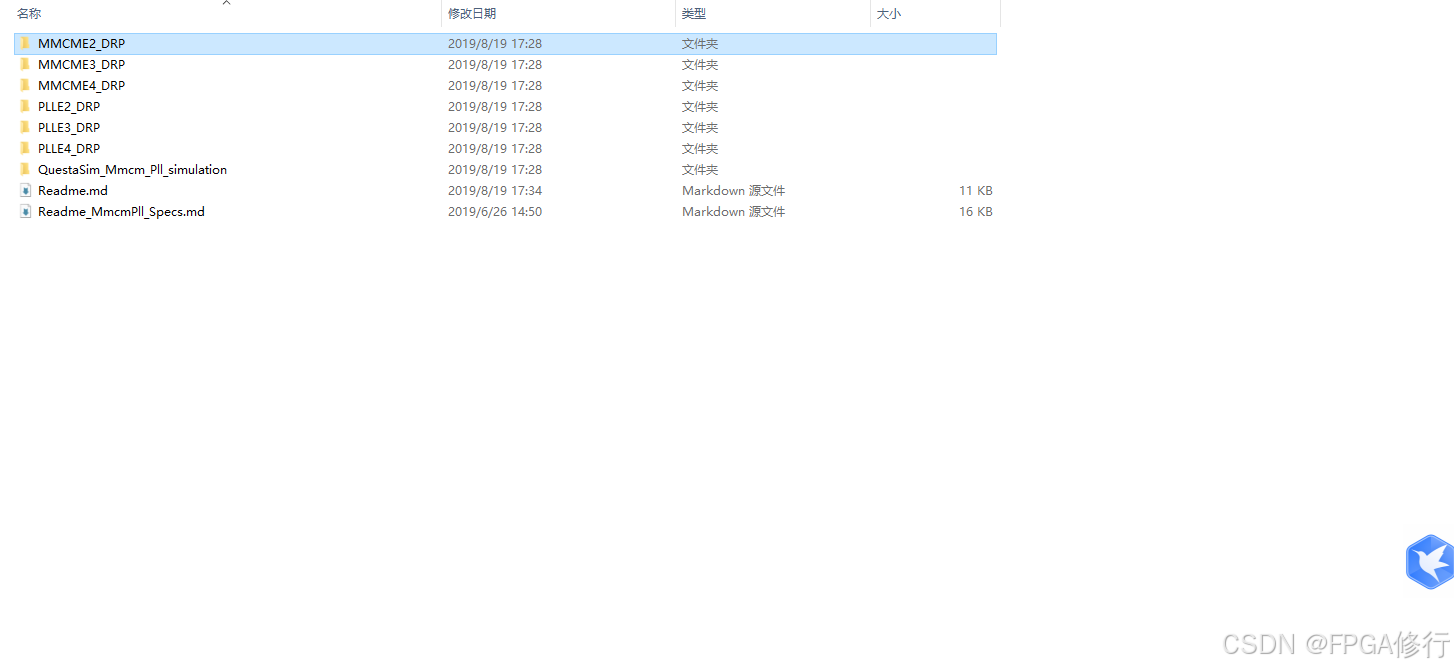
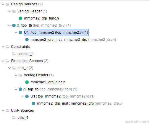
打开下载的压缩包我们可以看到MMCME2_DRP、MMCME3_DRP、MMCME4_DRP,这些是在不同器件上使用的。根据你使用的那个系列的芯片进行选择。我们这里使用的是XC7K325TFFG900,所以选择MMCM2_DRP。
-
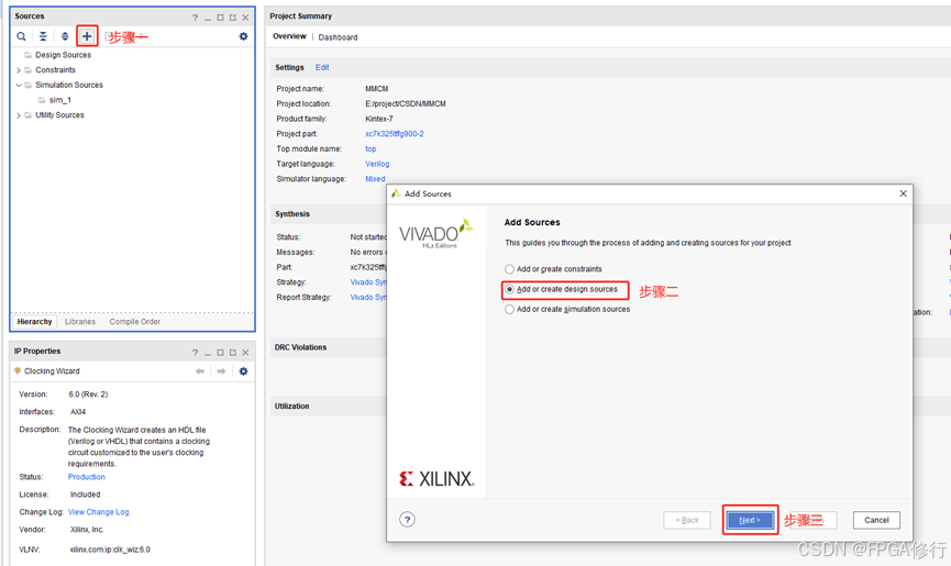
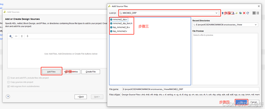
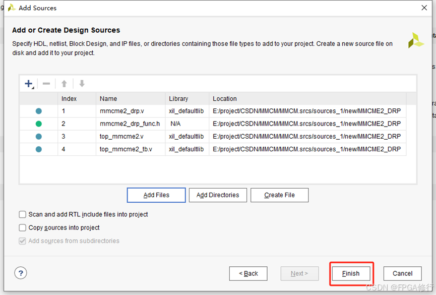
新建一个工程,将文件夹里的文件全部导入工程中。
-
其中mmcme2_drp_func.h是参数计算相关的函数,我们不用关心。top_tb是仿真文件。剩下的即是我们需要关心的地方。
-
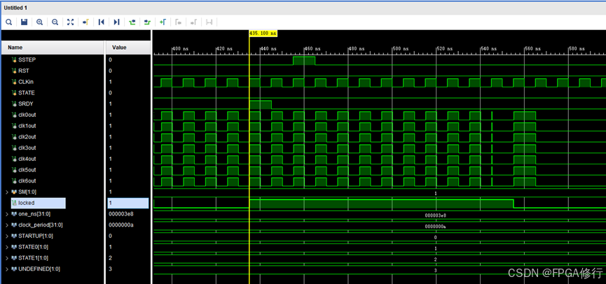
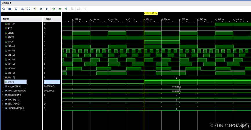
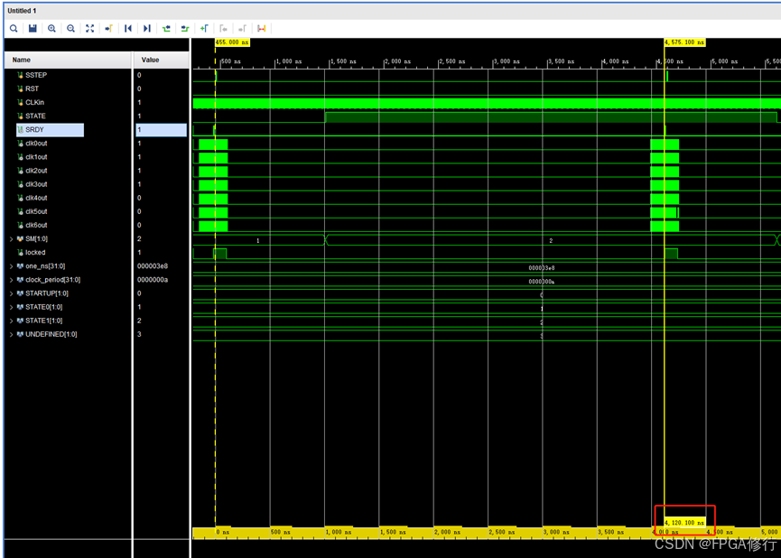
我们直接将这个工程进行仿真。可以看到时钟输出的频率发生改变。 且总耗时4120.1ns。
修改讲解
- 仿真文件。需要注意的是他的timescale是1ps。这个状态机很简单,就是当时钟锁定的时候拉高SSTEP一个脉冲,然后切换到下一个状态,锁定后又拉高切回上一个状态。这里表示的是在两种时钟配置下反复切换。
//-------------------------------------------------------------------------------------------
    localparam one_ns = 1000;
    localparam clock_period = 10;
    parameter [1:0]    STARTUP = 0, STATE0 = 1, STATE1 = 2, UNDEFINED = 3;
    reg [1:0] SM = STARTUP ;

always @ (posedge CLKin)
    begin
        if (RST)
               SM = STARTUP;
        else
            case (SM)
                STARTUP:
                    begin
                        SM = STATE0;
                        SSTEP=1'b0;
                        STATE=1'b0;
                    end
                STATE0:
                    begin
                        if (locked == 1 )
                            begin
                                #(1 * clock_period * one_ns) SSTEP= 1'b1;
                                #(1 * clock_period * one_ns) SSTEP=1'b0;
                                #(100 * clock_period * one_ns) SM = STATE1 ;
                                STATE=1'b1;
                            end
                    end
                STATE1:
                    begin
                        if (locked == 1 )
                            begin
                                #(1 * clock_period * one_ns) SSTEP= 1'b1;
                                #(1 * clock_period * one_ns) SSTEP=1'b0;
                                #(100 * clock_period * one_ns) SM = STATE0;
                                STATE=1'b0;
                            end
                    end
                UNDEFINED:   SM= STARTUP;
            endcase
        end
//
- top_mmcme2。这一部分看起来很多,但是了解几个关键点后,就可以顺利的使用起来了。并且这是我们在调用MMCM时的顶层模块。也就是修改里边的参数后,我们最终只需要对它顶层的四个参数进行控制就可以完成时钟配置的切换了。SSTEP、STATE、SRDY、locked。
//------------------------------------------------------------------------------------------
//   ____  ____
//  /   /\/   /
// /___/  \  /
// \   \   \/    � Copyright 2019 Xilinx, Inc. All rights reserved.
//  \   \        This file contains confidential and proprietary information of Xilinx, Inc.
//  /   /        and is protected under U.S. and international copyright and other
// /___/   /\    intellectual property laws.
// \   \  /  \
//  \___\/\___\
//
//-------------------------------------------------------------------------------------------
// Device:              7-Series
// Author:              Tatsukawa, Kruger, Defossez
// Entity Name:         top_mmcme2
// Purpose:             This is a basic demonstration of the MMCM_DRP
//                      connectivity to the MMCM_ADV.
// Tools:               Vivado_2019.1 or newer
// Limitations:
//
// Vendor:              Xilinx Inc.
// Version:             1.40
// Filename:            top_mmcme2.v
// Date Created:        30-Jul-2014
// Date Last Modified:  25-Jun-2019
//-------------------------------------------------------------------------------------------
// Disclaimer:
//		This disclaimer is not a license and does not grant any rights to the materials
//		distributed herewith. Except as otherwise provided in a valid license issued to you
//		by Xilinx, and to the maximum extent permitted by applicable law: (1) THESE MATERIALS
//		ARE MADE AVAILABLE "AS IS" AND WITH ALL FAULTS, AND XILINX HEREBY DISCLAIMS ALL
//		WARRANTIES AND CONDITIONS, EXPRESS, IMPLIED, OR STATUTORY, INCLUDING BUT NOT LIMITED
//		TO WARRANTIES OF MERCHANTABILITY, NON-INFRINGEMENT, OR FITNESS FOR ANY PARTICULAR
//		PURPOSE; and (2) Xilinx shall not be liable (whether in contract or tort, including
//		negligence, or under any other theory of liability) for any loss or damage of any
//		kind or nature related to, arising under or in connection with these materials,
//		including for any direct, or any indirect, special, incidental, or consequential
//		loss or damage (including loss of data, profits, goodwill, or any type of loss or
//		damage suffered as a result of any action brought by a third party) even if such
//		damage or loss was reasonably foreseeable or Xilinx had been advised of the
//		possibility of the same.
//
// CRITICAL APPLICATIONS
//		Xilinx products are not designed or intended to be fail-safe, or for use in any
//		application requiring fail-safe performance, such as life-support or safety devices
//		or systems, Class III medical devices, nuclear facilities, applications related to
//		the deployment of airbags, or any other applications that could lead to death,
//		personal injury, or severe property or environmental damage (individually and
//		collectively, "Critical Applications"). Customer assumes the sole risk and
//		liability of any use of Xilinx products in Critical Applications, subject only to
//		applicable laws and regulations governing limitations on product liability.
//
// THIS COPYRIGHT NOTICE AND DISCLAIMER MUST BE RETAINED AS PART OF THIS FILE AT ALL TIMES.
//
// Contact:    e-mail  hotline@xilinx.com        phone   + 1 800 255 7778
//-------------------------------------------------------------------------------------------
// Revision History:
//  Rev: 30-Apr-2014 - Tatsukawa
//      Initial code release
//  Rev: 25-Jun-2019 - Defossez
//      Add possibility to register the LOCKED signal.
//-------------------------------------------------------------------------------------------
//
`timescale 1ps/1ps
//
//-------------------------------------------------------------------------------------------
// Entity pin description
//-------------------------------------------------------------------------------------------
// Inputs
//      SSTEP:      Start a reconfiguration. It should only be pulsed for one clock cycle.
//      STATE:      Determines which state the MMCM_ADV will be reconfigured to. A value
//                  of 0 correlates to state 1, and a value of 1 correlates to state 2.
//      RST:        RST will reset the entire reference design including the MMCM_ADV.
//      CLKIN:      Clock for the MMCM_ADV CLKIN as well as the clock for the MMCM_DRP module
//      SRDY:       Pulses for one clock cycle after the MMCM_ADV is locked and the
//                  MMCM_DRP module is ready to start another re-configuration.
// Outputs
//      LOCKED_OUT: MMCM is locked after configuration or reconfiguration.
//      CLK0OUT:    These are the clock outputs from the MMCM_ADV.
//      CLK1OUT:    These are the clock outputs from the MMCM_ADV.
//      CLK2OUT:    These are the clock outputs from the MMCM_ADV.
//      CLK3OUT:    These are the clock outputs from the MMCM_ADV.
//      CLK4OUT:    These are the clock outputs from the MMCM_ADV.
//      CLK5OUT:    These are the clock outputs from the MMCM_ADV.
//      CLK6OUT:    These are the clock outputs from the MMCM_ADV.
//-------------------------------------------------------------------------------------------
module top_mmcme2
    (
        input    SSTEP,
        input    STATE,
        input    RST,
        input    CLKIN,
        output   SRDY,
 		output 	 LOCKED_OUT,
        output   CLK0OUT,
        output   CLK1OUT,
        output   CLK2OUT,
        output   CLK3OUT,
        output   CLK4OUT,
        output   CLK5OUT,
        output   CLK6OUT
    );
//-------------------------------------------------------------------------------------------
// These signals are used as direct connections between the MMCM_ADV and the
// MMCM_DRP.
(* mark_debug = "true" *) wire [15:0]    di;
(* mark_debug = "true" *) wire [6:0]     daddr;
(* mark_debug = "true" *) wire [15:0]    dout;
(* mark_debug = "true" *) wire           den;
(* mark_debug = "true" *) wire           dwe;
wire            dclk;
wire            rst_mmcm;
wire            drdy;
reg				current_state;
reg [7:0]		sstep_int ;
reg				init_drp_state = 1;
// These signals are used for the BUFG's necessary for the design.
wire            CLKIN_ibuf;
wire            clkin_bufgout;
wire            clkfb_bufgout;
wire            clkfb_bufgin;
wire            clk0_bufgin;
wire            clk0_bufgout;
wire            clk1_bufgin;
wire            clk1_bufgout;
wire            clk2_bufgin;
wire            clk2_bufgout;
wire            clk3_bufgin;
wire            clk3_bufgout;
wire            clk4_bufgin;
wire            clk4_bufgout;
wire            clk5_bufgin;
wire            clk5_bufgout;
wire            clk6_bufgin;
wire            clk6_bufgout;
wire            LOCKED;
//-------------------------------------------------------------------------------------------
assign CLKIN_ibuf = CLKIN;
//
BUFG BUFG_IN    (.O (clkin_bufgout),    .I (CLKIN_ibuf));
BUFG BUFG_FB    (.O (clkfb_bufgout),    .I (clkfb_bufgin));
BUFG BUFG_CLK0  (.O (clk0_bufgout),     .I (clk0_bufgin));
BUFG BUFG_CLK1  (.O (clk1_bufgout),     .I (clk1_bufgin));
BUFG BUFG_CLK2  (.O (clk2_bufgout),     .I (clk2_bufgin));
BUFG BUFG_CLK3  (.O (clk3_bufgout),     .I (clk3_bufgin));
BUFG BUFG_CLK4  (.O (clk4_bufgout),     .I (clk4_bufgin));
BUFG BUFG_CLK5  (.O (clk5_bufgout),     .I (clk5_bufgin));
BUFG BUFG_CLK6  (.O (clk6_bufgout),     .I (clk6_bufgin));
//
// ODDR registers used to output clocks
ODDR ODDR_CLK0 (.Q(CLK0OUT), .C(clk0_bufgout), .CE(1'b1), .D1(1'b1), .D2(1'b0), .R(RST), .S(1'b0));
ODDR ODDR_CLK1 (.Q(CLK1OUT), .C(clk1_bufgout), .CE(1'b1), .D1(1'b1), .D2(1'b0), .R(RST), .S(1'b0));
ODDR ODDR_CLK2 (.Q(CLK2OUT), .C(clk2_bufgout), .CE(1'b1), .D1(1'b1), .D2(1'b0), .R(RST), .S(1'b0));
ODDR ODDR_CLK3 (.Q(CLK3OUT), .C(clk3_bufgout), .CE(1'b1), .D1(1'b1), .D2(1'b0), .R(RST), .S(1'b0));
ODDR ODDR_CLK4 (.Q(CLK4OUT), .C(clk4_bufgout), .CE(1'b1), .D1(1'b1), .D2(1'b0), .R(RST), .S(1'b0));
ODDR ODDR_CLK5 (.Q(CLK5OUT), .C(clk5_bufgout), .CE(1'b1), .D1(1'b1), .D2(1'b0), .R(RST), .S(1'b0));
ODDR ODDR_CLK6 (.Q(CLK6OUT), .C(clk6_bufgout), .CE(1'b1), .D1(1'b1), .D2(1'b0), .R(RST), .S(1'b0));
//
// MMCM_ADV that reconfiguration will take place on
//
//  BANDWIDTH:              : "HIGH", "LOW" or "OPTIMIZED"
//  DIVCLK_DIVIDE           : Value from 1 to 106
//  CLKFBOUT_MULT_F         : Value from 2 to 64
//  CLKFBOUT_PHASE          :
//  CLKFBOUT_USE_FINE_PS    : "TRUE" or "FALSE",
//  CLKIN1_PERIOD           : Value from 0.968 to 100.000. Set the period (ns) of input clocks
//  REF_JITTER1             :
//  CLKIN2_PERIOD           :
//  REF_JITTER2             :
//  CLKOUT parameters:
//  DIVIDE                  : Value from 1 to 128
//  DUTY_CYCLE              : 0.01 to 0.99 - This is dependent on the divide value.
//  PHASE                   : 0.0 to 360.0 - This is dependent on the divide value.
//  USE_FINE_PS             : TRUE or FALSE
//  Misc parameters
//  COMPENSATION
//  STARTUP_WAIT
//
MMCME2_ADV #(
   .BANDWIDTH           ("OPTIMIZED"),
   .DIVCLK_DIVIDE       (1),
   .CLKFBOUT_MULT_F     (6),
   .CLKFBOUT_PHASE      (0.0),
   .CLKFBOUT_USE_FINE_PS("FALSE"),
   .CLKIN1_PERIOD       (10.000),
   .REF_JITTER1         (0.010),
   .CLKIN2_PERIOD       (10.000),
   .REF_JITTER2         (0.010),
   .CLKOUT0_DIVIDE_F    (6),
   .CLKOUT0_DUTY_CYCLE  (0.5),
   .CLKOUT0_PHASE       (0.0),
   .CLKOUT0_USE_FINE_PS ("FALSE"),
   .CLKOUT1_DIVIDE      (6),
   .CLKOUT1_DUTY_CYCLE  (0.5),
   .CLKOUT1_PHASE       (0.0),
   .CLKOUT1_USE_FINE_PS ("FALSE"),
   .CLKOUT2_DIVIDE      (6),
   .CLKOUT2_DUTY_CYCLE  (0.5),
   .CLKOUT2_PHASE       (0.0),
   .CLKOUT2_USE_FINE_PS ("FALSE"),
   .CLKOUT3_DIVIDE      (6),
   .CLKOUT3_DUTY_CYCLE  (0.5),
   .CLKOUT3_PHASE       (0.0),
   .CLKOUT3_USE_FINE_PS ("FALSE"),
   .CLKOUT4_DIVIDE      (6),
   .CLKOUT4_DUTY_CYCLE  (0.5),
   .CLKOUT4_PHASE       (0.0),
   .CLKOUT4_USE_FINE_PS ("FALSE"),
   .CLKOUT4_CASCADE     ("FALSE"),
   .CLKOUT5_DIVIDE      (6),
   .CLKOUT5_DUTY_CYCLE  (0.5),
   .CLKOUT5_PHASE       (0.0),
   .CLKOUT5_USE_FINE_PS ("FALSE"),
   .CLKOUT6_DIVIDE      (6),
   .CLKOUT6_DUTY_CYCLE  (0.5),
   .CLKOUT6_PHASE       (0.0),
   .CLKOUT6_USE_FINE_PS ("FALSE"),
   .COMPENSATION        ("ZHOLD"),
   .STARTUP_WAIT        ("FALSE")
) mmcme2_test_inst (
   .CLKFBOUT            (clkfb_bufgin),
   .CLKFBOUTB           (),
   .CLKFBSTOPPED        (),
   .CLKINSTOPPED        (),
   .CLKOUT0             (clk0_bufgin),
   .CLKOUT0B            (),
   .CLKOUT1             (clk1_bufgin),
   .CLKOUT1B            (),
   .CLKOUT2             (clk2_bufgin),
   .CLKOUT2B            (),
   .CLKOUT3             (clk3_bufgin),
   .CLKOUT3B            (),
   .CLKOUT4             (clk4_bufgin),
   .CLKOUT5             (clk5_bufgin),
   .CLKOUT6             (clk6_bufgin),
   .DO                  (dout),
   .DRDY                (drdy),
   .DADDR               (daddr),
   .DCLK                (dclk),
   .DEN                 (den),
   .DI                  (di),
   .DWE                 (dwe),
   .LOCKED              (LOCKED),
   .CLKFBIN             (clkfb_bufgout),
   .CLKIN1              (clkin_bufgout),
   .CLKIN2              (),
   .CLKINSEL            (1'b1),
   .PSDONE              (),
   .PSCLK               (1'b0),
   .PSEN                (1'b0),
   .PSINCDEC            (1'b0),
   .PWRDWN              (1'b0),
   .RST                 (rst_mmcm)
);
// MMCM_DRP instance that will perform the reconfiguration operations
mmcme2_drp #(
    // Register the LOCKED signal with teh MMCME3_ADV input clock.
    // The LOCKED_IN (LOCKED from the MMCME3_ADV) is fed into a register and then
    // passed the LOCKED_OUT when REGISTER_LOCKED is set to "Reg" or when set to
    // "NoReg" LOCKED_IN is just passed on to LOCKED_OUT without being registered.
    .REGISTER_LOCKED       ("Reg"),
    // Use the registered LOCKED signal from the MMCME3 also for the DRP state machine.
    .USE_REG_LOCKED        ("No"),
    // Possible combination of above two parameters:
    // | REGISTER_LOCKED | USE_REG_LOCKED |                                            |
    // |-----------------|----------------|--------------------------------------------|
    // |      "NoReg"    |     "No"       | LOCKED is just passed through mmcme3_drp   |
    // |                 |                | and is used as is with the state machine   |
    // |      "NoReg"    |     "Yes"      | NOT ALLOWED                                |
    // |       "Reg"     |     "No"       | LOCKED is registered but the unregistered  |
    // |                 |                | version is used for the state machine.     |
    // |       "Reg"     |     "Yes"      | LOCKED is registered and the registered    |
    // |                 |                | version is also used by the state machine. |
    //
    //***********************************************************************
    // State 1 Parameters - These are for the first reconfiguration state.
    //***********************************************************************
    // Set the multiply to 6.0 with 0 deg phase offset, optimized bandwidth, input divide of 1
    .S1_CLKFBOUT_MULT(3),
    .S1_CLKFBOUT_PHASE(000_000),
    .S1_CLKFBOUT_FRAC(000),
    .S1_CLKFBOUT_FRAC_EN(0),
    .S1_BANDWIDTH("OPTIMIZED"),
    .S1_DIVCLK_DIVIDE(1),
    // Set clockout0 to a divide of 6.0 (unity gain), 0 deg phase offset, 50/50 duty cycle
    .S1_CLKOUT0_DIVIDE(6),
    .S1_CLKOUT0_PHASE(000_000),
    .S1_CLKOUT0_DUTY(50000),
    .S1_CLKOUT0_FRAC(000),
    .S1_CLKOUT0_FRAC_EN(0),
    // Set clockout 1 to a divide of 1, 0 deg phase offset, 50/50 duty cycle
    .S1_CLKOUT1_DIVIDE(1),
    .S1_CLKOUT1_PHASE(000_000),
    .S1_CLKOUT1_DUTY(50000),
    // Set clockout 2 to a divide of 2, 0 deg phase offset, 50/50 duty cycle
    .S1_CLKOUT2_DIVIDE(2),
    .S1_CLKOUT2_PHASE(000_000),
    .S1_CLKOUT2_DUTY(50000),
    // Set clockout 3 to a divide of 3, 0 deg phase offset, 50/50 duty cycle
    .S1_CLKOUT3_DIVIDE(3),
    .S1_CLKOUT3_PHASE(000_000),
    .S1_CLKOUT3_DUTY(50000),
    // Set clockout 4 to a divide of 4, 0 deg phase offset, 50/50 duty cycle
    .S1_CLKOUT4_DIVIDE(4),
    .S1_CLKOUT4_PHASE(000_000),
    .S1_CLKOUT4_DUTY(50000),
    // Set clockout 5 to a divide of 5, 0 deg phase offset, 50/50 duty cycle
    .S1_CLKOUT5_DIVIDE(5),
    .S1_CLKOUT5_PHASE(000_000),
    .S1_CLKOUT5_DUTY(50000),
    // Set clockout 6 to a divide of 10, 0 deg phase offset, 50/50 duty cycle
    .S1_CLKOUT6_DIVIDE(10),
    .S1_CLKOUT6_PHASE(000_000),
    .S1_CLKOUT6_DUTY(50000),
    //***********************************************************************
    // State 2 Parameters - These are for the second reconfiguration state.
    //***********************************************************************
    .S2_CLKFBOUT_MULT(7),
    .S2_CLKFBOUT_PHASE(000_000),
    .S2_CLKFBOUT_FRAC(000),
    .S2_CLKFBOUT_FRAC_EN(0),
    .S2_BANDWIDTH("OPTIMIZED"),
    .S2_DIVCLK_DIVIDE(1),
    // Set clockout 0 to a divide of 4.750, 0 deg phase offset, 50/50 duty cycle
    .S2_CLKOUT0_DIVIDE(7),
    .S2_CLKOUT0_PHASE(000_000),
    .S2_CLKOUT0_DUTY(50000),
    .S2_CLKOUT0_FRAC(000),
    .S2_CLKOUT0_FRAC_EN(0),
    // Set clockout 1 to a divide of 1, 45.0 deg phase offset, 50/50 duty cycle
    .S2_CLKOUT1_DIVIDE(1),
    .S2_CLKOUT1_PHASE(045_000),
    .S2_CLKOUT1_DUTY(50000),
    // Set clock out 0 to a divide of 1, 90.0 deg phase offset, 50/50 duty cycle
    .S2_CLKOUT2_DIVIDE(1),
    .S2_CLKOUT2_PHASE(090_000),
    .S2_CLKOUT2_DUTY(90000),
    // Set clockout3 to a divide of 1, 135.0 deg phase offset, 50/50 duty cycle
    .S2_CLKOUT3_DIVIDE(1),
    .S2_CLKOUT3_PHASE(135_000),
    .S2_CLKOUT3_DUTY(50000),
    // Set clockout4 to a divide of 1, 180.0 deg phase offset, 50/50 duty cycle
    .S2_CLKOUT4_DIVIDE(1),
    .S2_CLKOUT4_PHASE(180_000),
    .S2_CLKOUT4_DUTY(50000),
    // Set clockout5 to a divide of 1, 225.0 deg phase offset, 50/50 duty cycle
    .S2_CLKOUT5_DIVIDE(1),
    .S2_CLKOUT5_PHASE(225_000),
    .S2_CLKOUT5_DUTY(50000),
    // Set clockout6 to a divide of 1, 270.0 deg phase offset, 50/50 duty cycle
    .S2_CLKOUT6_DIVIDE(1),
    .S2_CLKOUT6_PHASE(270_000),
    .S2_CLKOUT6_DUTY(50000)
) mmcme2_drp_inst (
    .SADDR              (STATE),
    .SEN                (sstep_int[0]),
    .RST                (RST),
    .SRDY               (SRDY),
    .SCLK               (clkin_bufgout),
    .DO                 (dout),
    .DRDY               (drdy),
    .LOCK_REG_CLK_IN    (clkin_bufgout),
    .LOCKED_IN          (LOCKED),
    .DWE                (dwe),
    .DEN                (den),
    .DADDR              (daddr),
    .DI                 (di),
    .DCLK               (dclk),
    .RST_MMCM           (rst_mmcm),
    .LOCKED_OUT         (LOCKED_OUT)
);
   //***********************************************************************
   // Additional STATE and SSTEP logic for push buttons and switches
   //***********************************************************************
// The following logic is not required but is being used to allow the DRP
// circuitry work more effectively with boards that use toggle switches or
// buttons that may not adhere to the single clock requirement.
//
// Only start DRP after initial lock and when STATE has changed
always @ (posedge clkin_bufgout or posedge SSTEP)
    if (SSTEP) sstep_int <=  8'h80;
    else sstep_int <= {1'b0, sstep_int[7:1]};
//
//-------------------------------------------------------------------------------------------
endmodule
- 上面顶层代码中,截出来这一部分就是我们需要修改的参数了。其中
State 1 Parameters - These are for the first reconfiguration state.
State 1 Parameters - These are for the first reconfiguration state.
是两个状态,仿真文件里切换的就是这两个。
公式:VCO Frequency = (Input Clock Frequency) * (CLKFBOUT_MULT)/DIVCLK_DIVIDE
CLKFBOUT_MULT:This attribute modifies the input clock multiplier to change the VCO output frequency of the MMCM.
DIVCLK_DIVIDE:Sets the divide value for the DIVCLK output.
CLKFBOUT_PHASE:相位移动。如果有需要可以按照整数值乘以1000。例如,45°的相移将是45,000.进行设置
CLKFBOUT_FRAC/CLKFBOUT_FRAC_EN:在需要小数乘法的时候使用。例如代码里默认CLKFBOUT_MULT=3、CLKFBOUT_FRAC/CLKFBOUT_FRAC_EN0、DIVCLK_DIVIDE1.那么VCO频率就等于VCO Frequency = (Input Clock Frequency) *3。
如果整数不能满足要求,则可以将CLKFBOUT_FRAC_EN设置为1、CLKFBOUT_FRAC设置为0-875范围内的数。那么公式将变为VCO Frequency = (Input Clock Frequency) *(CLKFBOUT_MULT+CLKFBOUT_FRAC/1000)/DIVCLK_DIVIDE;
上面这几个参数决定了MMCM内部VCO工作频率,往后所有的时钟输出频率均是由VCO频率分频出来的。
后面的参数就很简单了
DIVIDE:根据上面算出的VCO频率进行分频;
PHASE:相移;
DUTY:占空比,例如高点平占比60%,就设置为60,000;
FRAC:和CLKFBOUT_FRAC一眼,不过这里是除法;
FRAC_EN:设置为1时FRAC才会生效。
CLKOUT Frequency =( VCO Frequency )/(DIVIDE + FRAC/1000);
    //***********************************************************************
    // State 1 Parameters - These are for the first reconfiguration state.
    //***********************************************************************
    // Set the multiply to 6.0 with 0 deg phase offset, optimized bandwidth, input divide of 1
    .S1_CLKFBOUT_MULT(3),
    .S1_CLKFBOUT_PHASE(000_000),
    .S1_CLKFBOUT_FRAC(000),
    .S1_CLKFBOUT_FRAC_EN(0),
    .S1_BANDWIDTH("OPTIMIZED"),
    .S1_DIVCLK_DIVIDE(1),
    // Set clockout0 to a divide of 6.0 (unity gain), 0 deg phase offset, 50/50 duty cycle
    .S1_CLKOUT0_DIVIDE(6),
    .S1_CLKOUT0_PHASE(000_000),
    .S1_CLKOUT0_DUTY(50000),
    .S1_CLKOUT0_FRAC(000),
    .S1_CLKOUT0_FRAC_EN(0),
    // Set clockout 1 to a divide of 1, 0 deg phase offset, 50/50 duty cycle
    .S1_CLKOUT1_DIVIDE(1),
    .S1_CLKOUT1_PHASE(000_000),
    .S1_CLKOUT1_DUTY(50000),
    // Set clockout 2 to a divide of 2, 0 deg phase offset, 50/50 duty cycle
    .S1_CLKOUT2_DIVIDE(2),
    .S1_CLKOUT2_PHASE(000_000),
    .S1_CLKOUT2_DUTY(50000),
    // Set clockout 3 to a divide of 3, 0 deg phase offset, 50/50 duty cycle
    .S1_CLKOUT3_DIVIDE(3),
    .S1_CLKOUT3_PHASE(000_000),
    .S1_CLKOUT3_DUTY(50000),
    // Set clockout 4 to a divide of 4, 0 deg phase offset, 50/50 duty cycle
    .S1_CLKOUT4_DIVIDE(4),
    .S1_CLKOUT4_PHASE(000_000),
    .S1_CLKOUT4_DUTY(50000),
    // Set clockout 5 to a divide of 5, 0 deg phase offset, 50/50 duty cycle
    .S1_CLKOUT5_DIVIDE(5),
    .S1_CLKOUT5_PHASE(000_000),
    .S1_CLKOUT5_DUTY(50000),
    // Set clockout 6 to a divide of 10, 0 deg phase offset, 50/50 duty cycle
    .S1_CLKOUT6_DIVIDE(10),
    .S1_CLKOUT6_PHASE(000_000),
    .S1_CLKOUT6_DUTY(50000),
    //***********************************************************************
    // State 2 Parameters - These are for the second reconfiguration state.
    //***********************************************************************
    .S2_CLKFBOUT_MULT(7),
    .S2_CLKFBOUT_PHASE(000_000),
    .S2_CLKFBOUT_FRAC(000),
    .S2_CLKFBOUT_FRAC_EN(0),
    .S2_BANDWIDTH("OPTIMIZED"),
    .S2_DIVCLK_DIVIDE(1),
    // Set clockout 0 to a divide of 4.750, 0 deg phase offset, 50/50 duty cycle
    .S2_CLKOUT0_DIVIDE(7),
    .S2_CLKOUT0_PHASE(000_000),
    .S2_CLKOUT0_DUTY(50000),
    .S2_CLKOUT0_FRAC(000),
    .S2_CLKOUT0_FRAC_EN(0),
    // Set clockout 1 to a divide of 1, 45.0 deg phase offset, 50/50 duty cycle
    .S2_CLKOUT1_DIVIDE(1),
    .S2_CLKOUT1_PHASE(045_000),
    .S2_CLKOUT1_DUTY(50000),
    // Set clock out 0 to a divide of 1, 90.0 deg phase offset, 50/50 duty cycle
    .S2_CLKOUT2_DIVIDE(1),
    .S2_CLKOUT2_PHASE(090_000),
    .S2_CLKOUT2_DUTY(90000),
    // Set clockout3 to a divide of 1, 135.0 deg phase offset, 50/50 duty cycle
    .S2_CLKOUT3_DIVIDE(1),
    .S2_CLKOUT3_PHASE(135_000),
    .S2_CLKOUT3_DUTY(50000),
    // Set clockout4 to a divide of 1, 180.0 deg phase offset, 50/50 duty cycle
    .S2_CLKOUT4_DIVIDE(1),
    .S2_CLKOUT4_PHASE(180_000),
    .S2_CLKOUT4_DUTY(50000),
    // Set clockout5 to a divide of 1, 225.0 deg phase offset, 50/50 duty cycle
    .S2_CLKOUT5_DIVIDE(1),
    .S2_CLKOUT5_PHASE(225_000),
    .S2_CLKOUT5_DUTY(50000),
    // Set clockout6 to a divide of 1, 270.0 deg phase offset, 50/50 duty cycle
    .S2_CLKOUT6_DIVIDE(1),
    .S2_CLKOUT6_PHASE(270_000),
    .S2_CLKOUT6_DUTY(50000)
特别需要注意的是,不同器件的VCO支持的频率范围是有规定的,具体使用哪款器件可以查看相应的器件手册。在对输入时钟进行mult与divide时需要注意到这点,否则PLL不能锁定。相关的器件手册也为大家下载好了,有需要的自行下载即可。
总结
本片文章讲解了XAPP888提供的时钟重配置工具中一些简单的参数配置,第一次使用的工程师们可以下载对应的文件,修改内部参数仿真,加强理解。


 6759
6759

 被折叠的 条评论
为什么被折叠?
被折叠的 条评论
为什么被折叠?
 到【灌水乐园】发言


