


V-by-One电路设计
关于VbyOne接口,V-by-One HS是由日本赛恩电子公司(THine Electornics)开发的适用于平板显示器的信号传输接口标准。目前,广泛应用在多功能打印机等办公设备、车载娱乐设备、机器人、安防系统等领域。
1 优势
- 高速(支持最高4Gbps速率,有效数据速率达3.2Gbps)
- 低功耗(与固定的速率传输相比,传输速率可变)
- 低EMI(支持扰码和数据时钟恢复)
- 支持时钟对齐(时钟信号恢复技术,解决了在LVDS方案下日趋显著化的配线时滞问题)。
- 传输距离远,可达15米。
2 系统框图
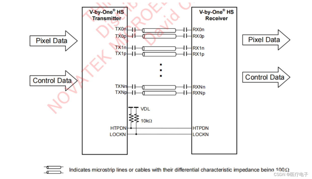
说明:
- TX和RX数据传输线两端需匹配去耦电容
- 在TX端控制信号LOCKN,HTPDN需上拉电阻。
- TX和RX之间传输线数量由色深和pixel clock决定。
- TX端控制信号有H-sync,V-sync,DE和CTL信号。
- 传输端支持预加重(pre-emphasis),接收端支持EQ均衡(equalizer)
2.1 Data Line数量选择
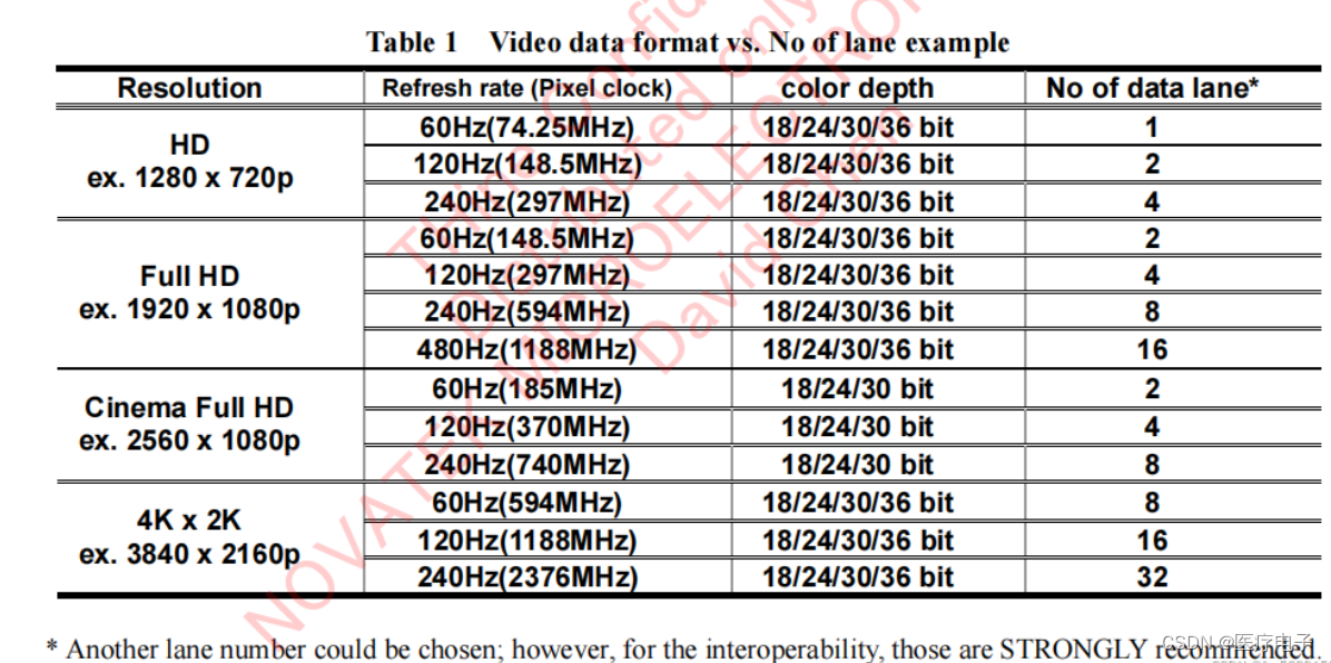
像素时钟计算Pixel Clock=H-totalV-totalrefresh rate
案 例:4K*2K 60Hz,Pixel Clock=4400 x 2250 x 60=594Mhz颜色深度计算:Color depth=R(6、8、10、12bit)+G(6、8、10、12bit)+B(6、8、10、
12bit)
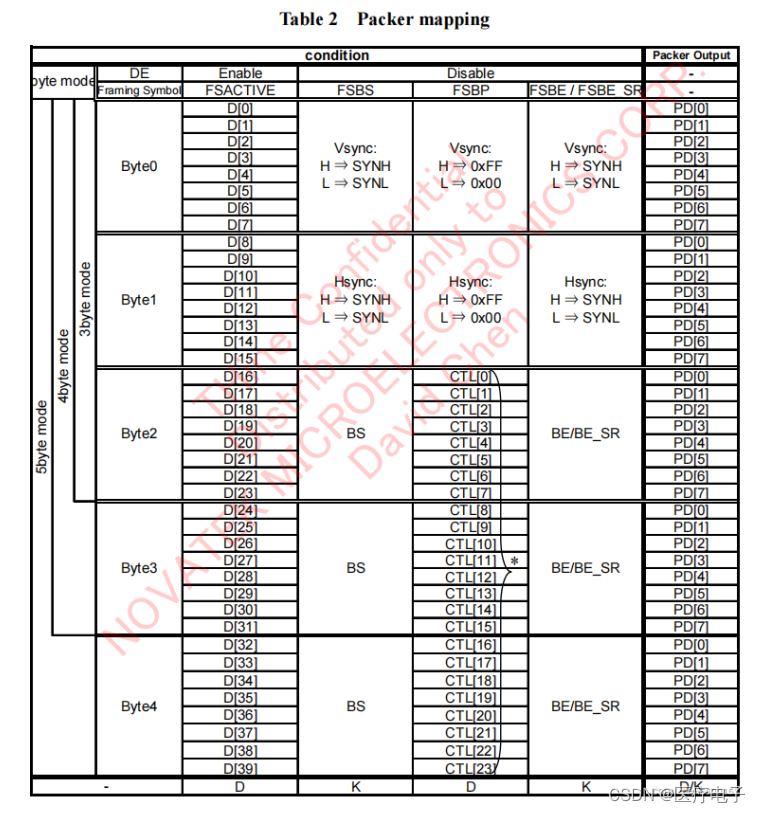
2.2 数据包字节模式选择
根据Color depth选取数据包字节模式byte mode,支持byte mode模式:3byte,4byte,5byte
举例:10bit色深,则一个pixel需要3(R,G,B)*10bit=30bit的数据,4byte mode可以支持,另外5byte mode也可以支持.


 466
466

 被折叠的 条评论
为什么被折叠?
被折叠的 条评论
为什么被折叠?
 到【灌水乐园】发言


