


 本文详细介绍了数字电路中的各种触发器与锁存器,包括D触发器、带复位功能的触发器、锁存器等,并通过Verilog代码示例展示了其工作原理与应用。还探讨了异步与同步复位的区别,以及如何使用触发器进行边沿检测。
80~触发器和锁存器
- 80.D flip-flop (Dff)
- 81.D flip-flops
- 82.DFF with reset (Dff8r)
- 83.DFF with reset value
- 84.DFF with asynchronous reset
- 85.DFF with byte enable
- 86.D latch(D锁存器)
- 87.DFF(异步)
- 88.DFF(同步)
- 89.DFF+gate
- 90.Mux and DFF
- 91.Mux and DFF
- 92.DFFS and gates
- 93.Create circuit from truth table
- 94.Detect an Edge
- 95.Detect both edges
- 96.Edge capture register
- 97.Dual-edge triggered flip-flop(没咋看懂)
强烈建议大家去看看HDLBits 中文导学,原文在知乎
链接: link.
从这里开始就要正式进入时序逻辑啦,难点来了;
80.D flip-flop (Dff)
D触发器:
- t1时刻: d -> 0;
- t2时刻: clk->1 上升沿到来,触发器存储的数据变成 0,输出 q 保持为存储的值:0,直到下一个时钟上升沿到来;
- t3时刻: d -> 1(d:我变了),q 仍保持 0 不动摇(时钟沿还没来呢);
- t4时刻: clk->1 上升沿到来,q->1(q:时钟沿来了,我该变身了)
module top_module(
	input clk,
	input d,
	output reg q);

	// Use non-blocking assignment for edge-triggered always blocks
	always @(posedge clk)
		q <= d;//非阻塞赋值

	// Undefined simulation behaviour can occur if there is more than one edge-triggered
	// always block and blocking assignment is used. Which always block is simulated first?

endmodule
81.D flip-flops
一样的
always@(posedge clk)begin
        q<=d;
    end
82.DFF with reset (Dff8r)
添加了一个复位信号
always@(posedge clk)begin
     if(reset)
     q<=8'b0;
     else
     q<=d;
 end
83.DFF with reset value
always@(negedge clk)begin
        if(reset)
            q<=8'h34;
        else
            q<=d;

    end
84.DFF with asynchronous reset
asynchronous reset:异步复位;
同步复位:当同步复位事件发生时,等到下一个时钟上升沿才会得到响应,响应的速度比较慢。
异步复位:响应很快,异步复位有效的时刻,复位响应就会发生,好像戳破气球一般。
直接将areset加入敏感元器件表中,
always@(posedge clk or posedge areset)begin
       if(areset)
            q <= 8'b0;
        else
    	    q <= d;
    end
85.DFF with byte enable
这一题其实还是有一点复杂的,直接照搬题目:
本题中需要创建一个 16 路 D触发器。使能端 ena 信号有效时,触发器在时钟上升沿工作。
byteena 使能信号以 byte 为单位管理 8 路触发器在时钟边沿触发与否。byteena [1] 作为 d[15:8] 高位字节的使能端,byteena [0] 则控制 d 的低位字节。
resetn 为同步,低电平有效复位信号。
所有的触发器在时钟上升沿被触发
module top_module (
    input clk,
    input resetn,
    input [1:0] byteena,
    input [15:0] d,
    output [15:0] q
);
    always@(posedge clk)begin
        if(~resetn)begin
            q<=16'd0;
        end
        else  if(byteena[0]||byteena[1])begin //这里的else必须要加,不加的话前面的复位信号不起作用
            if(byteena[0])
                q[7:0]<=d[7:0];
            if(byteena[1]) //这里不能写else语句,这个并不是二选一的语句,是可以同时成立的
            q[15:8]<=d[15:8];
        end
    end

endmodule
这里主要就是一个语句的结构层次的问题,复位和使能语句是并列二选一的,只能有一个同时生效,而使能语句下的高低位使能的语句是可以并列的;
86.D latch(D锁存器)
锁存器锁存的触发事件发生于使能端 ena 的电平;
module top_module (
    input d,
    input ena,
    output q);
    always@(*)
        if(ena)
        q<=d;
endmodule
87.DFF(异步)
module top_module (
    input clk,
    input d,
    input ar,   // asynchronous reset
    output q);
    always@(posedge clk or posedge ar)//将异步复位信号直接加入到敏感器件列表中
        if(ar)
            q<=1'b0;
    else
        q<=d;
endmodule
88.DFF(同步)
module top_module (
    input clk,
    input d,
    input r,   // synchronous reset
    output q);
    always@(posedge clk )
        if(r)
            q<=1'b0;
    else
        q<=d;
endmodule
89.DFF+gate
always@(posedge clk)
        out<=in^out;
90.Mux and DFF
这一题只是让实现其中的一个选择器加触发器的子模块
module top_module (
  input clk,
  input L,
  input r_in,
  input q_in,
  output reg Q);
  always@(posedge clk)
      Q<=L?r_in:q_in;

endmodule
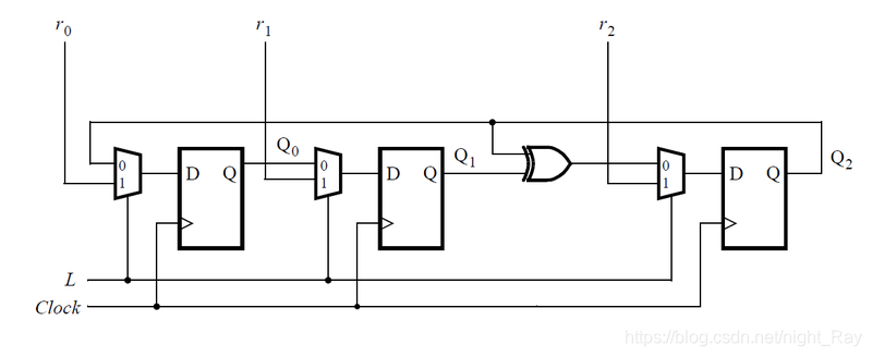
91.Mux and DFF

module top_module (
    input clk,
    input w, R, E, L,
    output Q
);
    wire m1,m2;
    assign m1= E?w:Q;
    assign m2= L?R:m1;


  /*  always@(posedge clk)
        m1= E?w:Q;
        Q<= L?R:m1;
        直接用两个非阻塞赋值就会报错,不知道为什么
*/


    always@(posedge clk)
     Q<=m2;
endmodule
92.DFFS and gates

module top_module (
    input clk,
    input x,
    output z
);
    reg q1=0,q2=0,q3=0; //开始用的wire,会报错
    always@(posedge clk)
        q1<=q1^x;
    always@(posedge clk)
        q2<=x&(~q2);
    always@(posedge clk)
        q3<=x|(~q3);

    assign z=~(q1|q2|q3);

endmodule
93.Create circuit from truth table
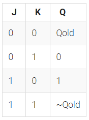
module top_module (
    input clk,
    input j,
    input k,
    output Q);
    always@(posedge clk)
        case({j,k})
            2'b00:Q<=Q;
            2'b01:Q<=0;
            2'b10:Q<=1;
            2'b11:Q<=!Q;
        endcase

endmodule
94.Detect an Edge
link.
边沿检测:说实话,看了几遍,看的不是太懂。大概的意思就是,引入一个寄存器,这个寄存器的输入信号是上一个时钟信号的输入,然后输出是这个时钟的输入,然后比较的话,因为有延迟,这个时钟的信号在上个时钟之后变成0,就是下降沿。
module top_module (
    input clk,
    input [7:0] in,
    output [7:0] pedge
);
    reg[7:0] temp;  //寄存器类型的信号
    always@(posedge clk)
        begin
        temp <=in;
       //temp在时钟到来的时候时钟保存上个时钟的in
        pedge <= ~temp & in;
      //如果这个时钟为1,上个时钟为0,说明上升沿
       end
    //这边的begin,end没加会报错,不清楚是什么原因

endmodule
95.Detect both edges
只要时钟信号和上个时钟不一样,就可以0判断,直接用异或就行;
module top_module (
    input clk,
    input [7:0] in,
    output [7:0] anyedge
);
    reg [7:0] temp;
    always@(posedge clk)
        begin
      temp <=in;
      anyedge <=temp^in;
        end
endmodule
96.Edge capture register
capture:捕获的意思就是,当获取到摸个信号之后保持不变,
module top_module (
    input clk,
    input reset,
    input [31:0] in,
    output [31:0] out
);
    reg[31:0] temp;
    reg[31:0] pos;//上升沿捕获标志
    //先来判断上升沿
    always@(posedge clk)
    begin
        temp<=in;
    end

     assign pos=temp &~in;
    //这里是看了解析才发现的,如果将这三个写在一个时序里会发生时序错误,
    always@(posedge clk)begin
        if(reset)
          out<=0;
        else
            for(int i=0;i<=31;i++)
                if(pos[i]==1)
    //这里必须要用一个for循环来判断pos的每一个位是否为1
                    out[i]<=1;

    end
endmodule
97.Dual-edge triggered flip-flop(没咋看懂)
这个时序图压根就看不懂;经过我的观察,应该是这样的,
时钟上升的时候q和d相反,时钟下降,q和d相同;
link看了一点这个,还是不怎么明白;所以就直接先过了;


 1698
1698

 被折叠的 条评论
为什么被折叠?
被折叠的 条评论
为什么被折叠?
 到【灌水乐园】发言


