


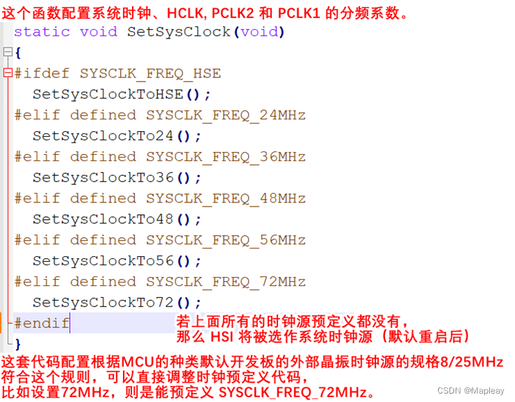
系统主干时钟
在system_stm32f10x.c文件中:
重要注意:
- 每次设备复位后,HSI用于系统的时钟源。
- 确保所选的系统时钟不要超过设备的最大时钟频率。
- 如果没有任何相关预定义,那么HSI将被用作系统默认时钟源。
- 在system_stm32f10x.c中系统时钟配置函数默认如下规则:
- For Low, Medium and High density Value line devices an external 8MHz crystal is used to drive the System clock.
- For Low, Medium and High density devices an external 8MHz crystal is used to drive the System clock.
- For Connectivity line devices an external 25MHz crystal is used to drive the System clock.
- 如果你使用了不同的外部晶振源,那么你必须正确地适配它。
#if defined (STM32F10X_LD_VL) || (defined STM32F10X_MD_VL) || (defined STM32F10X_HD_VL)
/* #define SYSCLK_FREQ_HSE HSE_VALUE */
#define SYSCLK_FREQ_24MHz 24000000
#else
/* #define SYSCLK_FREQ_HSE HSE_VALUE */
/* #define SYSCLK_FREQ_24MHz 24000000 */
/* #define SYSCLK_FREQ_36MHz 36000000 */
/* #define SYSCLK_FREQ_48MHz 48000000 */
/* #define SYSCLK_FREQ_56MHz 56000000 */
#define SYSCLK_FREQ_72MHz 72000000
#endif
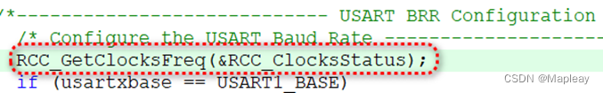
上面这些设置了系统时钟和各个总线的时钟频率,如果我们需要配置外设的时钟输入(比如USART),那么在对应的外设库函数c文件(stm32f10x_usart.c)中有相关函数调用函数RCC_GetClocksFreq(xxx)获取该外设直接的注入时钟源的数值。最后结合外设的输入时钟源与外设的配置方案,算得数值写入先关寄存器。(见下图USART1的配置)
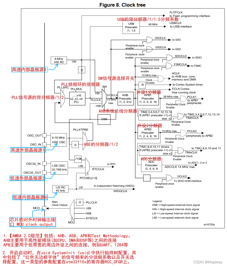
系统主干时钟是比喻的描述方法,包括了系统的物理输入时钟源,系统时钟和各种总线时钟的分频系数配置。
系统枝叶时钟也是比喻的描述方法,包括了系统各个片上外设(USART/CAN/DAC/ADC/USB/等)的由半导体厂商开发设计的硬件模块的配置系统参数配置。
下面就是以USART为例承上启下的案例分析。
系统枝叶时钟(USARTx时钟配置)
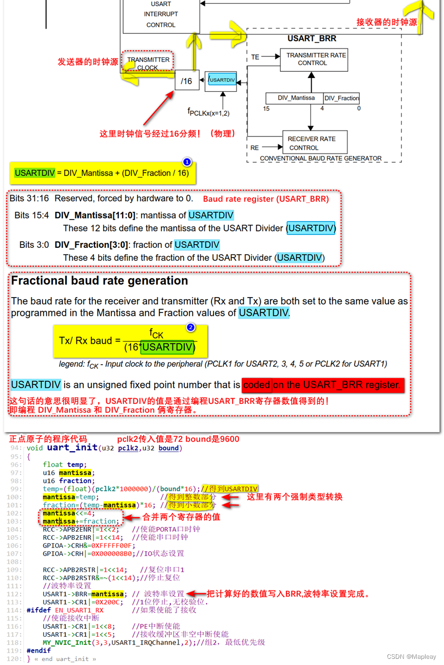
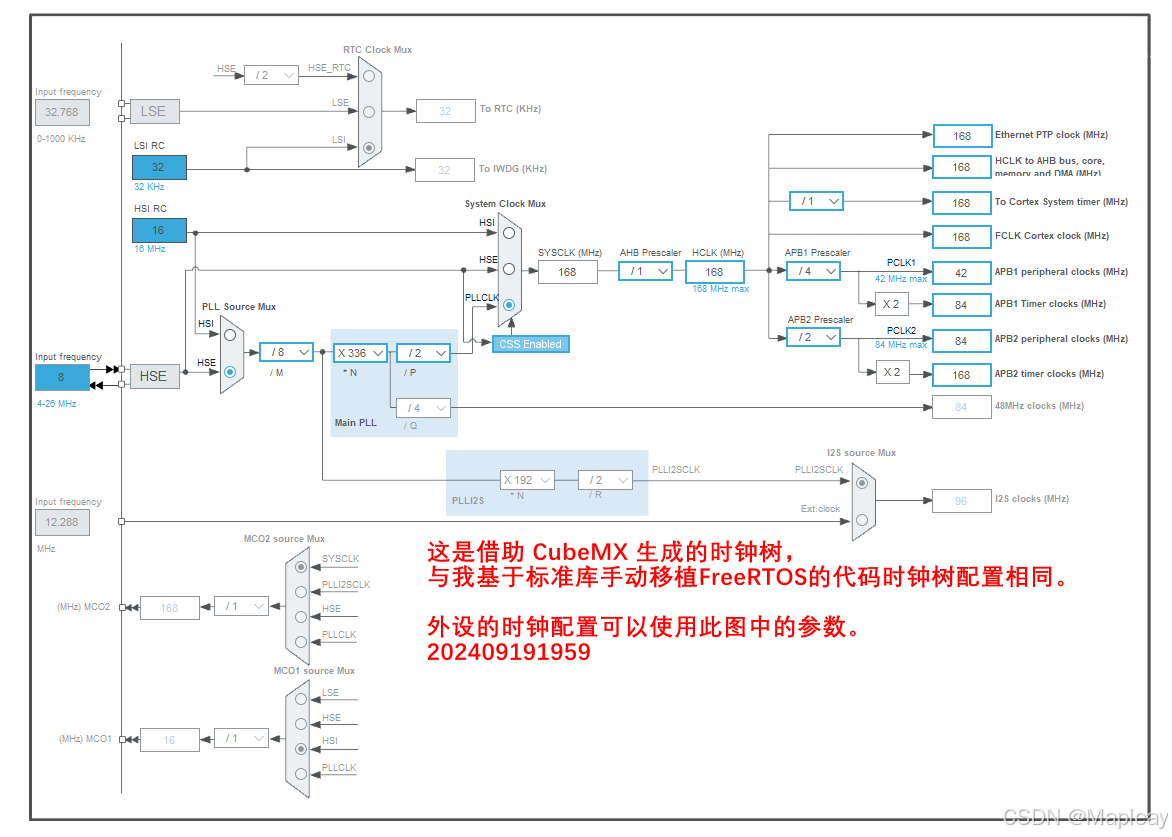
下面是系统时钟树的总图
配置USART的波特率寄存器
板载HSE为8MHz. 基于stm32f407vet6的标准外设库
void USART_Init(USART_TypeDef* USARTx, USART_InitTypeDef* USART_InitStruct)
{
  uint32_t tmpreg = 0x00, apbclock = 0x00;
  uint32_t integerdivider = 0x00;
  uint32_t fractionaldivider = 0x00;
  RCC_ClocksTypeDef RCC_ClocksStatus;

/*---------------------------- USART CR2 Configuration -----------------------*/
  tmpreg = USARTx->CR2;

  /* Clear STOP[13:12] bits */
  tmpreg &= (uint32_t)~((uint32_t)USART_CR2_STOP);

  /* Configure the USART Stop Bits, Clock, CPOL, CPHA and LastBit :
      Set STOP[13:12] bits according to USART_StopBits value */
  tmpreg |= (uint32_t)USART_InitStruct->USART_StopBits;

  /* Write to USART CR2 */
  USARTx->CR2 = (uint16_t)tmpreg;

/*---------------------------- USART CR1 Configuration -----------------------*/
  tmpreg = USARTx->CR1;

  /* Clear M, PCE, PS, TE and RE bits */
  tmpreg &= (uint32_t)~((uint32_t)CR1_CLEAR_MASK);

  /* Configure the USART Word Length, Parity and mode:
     Set the M bits according to USART_WordLength value
     Set PCE and PS bits according to USART_Parity value
     Set TE and RE bits according to USART_Mode value */
  tmpreg |= (uint32_t)USART_InitStruct->USART_WordLength | USART_InitStruct->USART_Parity |
            USART_InitStruct->USART_Mode;

  /* Write to USART CR1 */
  USARTx->CR1 = (uint16_t)tmpreg;

/*---------------------------- USART CR3 Configuration -----------------------*/
  tmpreg = USARTx->CR3;

  /* Clear CTSE and RTSE bits */
  tmpreg &= (uint32_t)~((uint32_t)CR3_CLEAR_MASK);

  /* Configure the USART HFC :
      Set CTSE and RTSE bits according to USART_HardwareFlowControl value */
  tmpreg |= USART_InitStruct->USART_HardwareFlowControl;

  /* Write to USART CR3 */
  USARTx->CR3 = (uint16_t)tmpreg;

/*---------------------------- USART BRR Configuration -----------------------*/
  /* 第一步 获取USARTx所在总线上的信号频率 apbclock */
  RCC_GetClocksFreq(&RCC_ClocksStatus);

  if ((USARTx == USART1) || (USARTx == USART6))
  {
    apbclock = RCC_ClocksStatus.PCLK2_Frequency;
  }
  else
  {
    apbclock = RCC_ClocksStatus.PCLK1_Frequency;
  }

  /* 第二步 计算USARTx波特率寄存器的整数值部分 */
  if ((USARTx->CR1 & USART_CR1_OVER8) != 0)
  {
    /* Integer part computing in case Oversampling mode is 8 Samples */
    integerdivider = ((25 * apbclock) / (2 * (USART_InitStruct->USART_BaudRate)));
  }
  else /* if ((USARTx->CR1 & USART_CR1_OVER8) == 0) */
  {
    /* Integer part computing in case Oversampling mode is 16 Samples */
    integerdivider = ((25 * apbclock) / (4 * (USART_InitStruct->USART_BaudRate)));
  }
  tmpreg = (integerdivider / 100) << 4;

  /* 第三步 计算USARTx波特率寄存器的小数值部分 */
  fractionaldivider = integerdivider - (100 * (tmpreg >> 4));

  /* Implement the fractional part in the register */
  if ((USARTx->CR1 & USART_CR1_OVER8) != 0)
  {
    tmpreg |= ((((fractionaldivider * 8) + 50) / 100)) & ((uint8_t)0x07);
  }
  else /* if ((USARTx->CR1 & USART_CR1_OVER8) == 0) */
  {
    tmpreg |= ((((fractionaldivider * 16) + 50) / 100)) & ((uint8_t)0x0F);
  }

  /* 第四步 合并整数和小数部分的值,写入 USARTx 波特率寄存器 BRR register 中 */
  USARTx->BRR = (uint16_t)tmpreg;
}


  /**
  * @brief  Returns the frequencies of different on chip clocks; SYSCLK, HCLK,
  *         PCLK1 and PCLK2.
  *
  * @note   The system frequency computed by this function is not the real
  *         frequency in the chip. It is calculated based on the predefined
  *         constant and the selected clock source:
  * @note     If SYSCLK source is HSI, function returns values based on HSI_VALUE(*)
  * @note     If SYSCLK source is HSE, function returns values based on HSE_VALUE(**)
  * @note     If SYSCLK source is PLL, function returns values based on HSE_VALUE(**)
  *           or HSI_VALUE(*) multiplied/divided by the PLL factors.
  * @note     (*) HSI_VALUE is a constant defined in stm32f4xx.h file (default value
  *               16 MHz) but the real value may vary depending on the variations
  *               in voltage and temperature.
  * @note     (**) HSE_VALUE is a constant defined in stm32f4xx.h file (default value
  *                25 MHz), user has to ensure that HSE_VALUE is same as the real
  *                frequency of the crystal used. Otherwise, this function may
  *                have wrong result.
  *
  * @note   The result of this function could be not correct when using fractional
  *         value for HSE crystal.
  *
  * @param  RCC_Clocks: pointer to a RCC_ClocksTypeDef structure which will hold
  *          the clocks frequencies.
  *
  * @note   This function can be used by the user application to compute the
  *         baudrate for the communication peripherals or configure other parameters.
  * @note   Each time SYSCLK, HCLK, PCLK1 and/or PCLK2 clock changes, this function
  *         must be called to update the structure's field. Otherwise, any
  *         configuration based on this function will be incorrect.
  *
  * @retval None
  */
void RCC_GetClocksFreq(RCC_ClocksTypeDef* RCC_Clocks)
{
  uint32_t tmp = 0, presc = 0, pllvco = 0, pllp = 2, pllsource = 0, pllm = 2;
#if defined(STM32F412xG) || defined(STM32F413_423xx) || defined(STM32F446xx)
  uint32_t pllr = 2;
#endif /* STM32F412xG || STM32F413_423xx || STM32F446xx */

  /* Get SYSCLK source -------------------------------------------------------*/
  tmp = RCC->CFGR & RCC_CFGR_SWS;

  switch (tmp)
  {
  case 0x00:  /* HSI used as system clock source */
    RCC_Clocks->SYSCLK_Frequency = HSI_VALUE;
    break;
  case 0x04:  /* HSE used as system clock  source */
    RCC_Clocks->SYSCLK_Frequency = HSE_VALUE;
    break;
  case 0x08:  /* PLL P used as system clock  source */

    /* PLL_VCO = (HSE_VALUE or HSI_VALUE / PLLM) * PLLN
    SYSCLK = PLL_VCO / PLLP
    */
    pllsource = (RCC->PLLCFGR & RCC_PLLCFGR_PLLSRC) >> 22;
    pllm = RCC->PLLCFGR & RCC_PLLCFGR_PLLM;

    if (pllsource != 0)
    {
      /* HSE used as PLL clock source */
      pllvco = (HSE_VALUE / pllm) * ((RCC->PLLCFGR & RCC_PLLCFGR_PLLN) >> 6);
    }
    else
    {
      /* HSI used as PLL clock source */
      pllvco = (HSI_VALUE / pllm) * ((RCC->PLLCFGR & RCC_PLLCFGR_PLLN) >> 6);
    }

    pllp = (((RCC->PLLCFGR & RCC_PLLCFGR_PLLP) >>16) + 1 ) *2;
    RCC_Clocks->SYSCLK_Frequency = pllvco/pllp;
    break;

  default:
    RCC_Clocks->SYSCLK_Frequency = HSI_VALUE;
    break;
  }
  /* Compute HCLK, PCLK1 and PCLK2 clocks frequencies ------------------------*/

  /* Get HCLK prescaler */
  tmp = RCC->CFGR & RCC_CFGR_HPRE;
  tmp = tmp >> 4;
  presc = APBAHBPrescTable[tmp];
  /* HCLK clock frequency */
  RCC_Clocks->HCLK_Frequency = RCC_Clocks->SYSCLK_Frequency >> presc;

  /* Get PCLK1 prescaler */
  tmp = RCC->CFGR & RCC_CFGR_PPRE1;
  tmp = tmp >> 10;
  presc = APBAHBPrescTable[tmp];
  /* PCLK1 clock frequency */
  RCC_Clocks->PCLK1_Frequency = RCC_Clocks->HCLK_Frequency >> presc;

  /* Get PCLK2 prescaler */
  tmp = RCC->CFGR & RCC_CFGR_PPRE2;
  tmp = tmp >> 13;
  presc = APBAHBPrescTable[tmp];
  /* PCLK2 clock frequency */
  RCC_Clocks->PCLK2_Frequency = RCC_Clocks->HCLK_Frequency >> presc;
}

/**
  * @brief  Setup the microcontroller system
  *         Initialize the Embedded Flash Interface, the PLL and update the
  *         SystemFrequency variable.
  * @param  None
  * @retval None
  */
void SystemInit(void)
{
  /* FPU settings ------------------------------------------------------------*/
  #if (__FPU_PRESENT == 1) && (__FPU_USED == 1)
    SCB->CPACR |= ((3UL << 10*2)|(3UL << 11*2));  /* set CP10 and CP11 Full Access */
  #endif
  /* Reset the RCC clock configuration to the default reset state ------------*/
  /* Set HSION bit */
  RCC->CR |= (uint32_t)0x00000001;

  /* Reset CFGR register */
  RCC->CFGR = 0x00000000;

  /* Reset HSEON, CSSON and PLLON bits */
  RCC->CR &= (uint32_t)0xFEF6FFFF;

  /* Reset PLLCFGR register */
  //RCC->PLLCFGR = 0x24003010; //原始版本
	RCC->PLLCFGR = 0x24005408;   //基于8MHz的HSE,设置SystemCoreClock = 168MHz的操作:调整PLLM、PLLN的分倍频系数。 v1.2.2。

  /* Reset HSEBYP bit */
  RCC->CR &= (uint32_t)0xFFFBFFFF;

  /* Disable all interrupts */
  RCC->CIR = 0x00000000;

#if defined(DATA_IN_ExtSRAM) || defined(DATA_IN_ExtSDRAM)
  SystemInit_ExtMemCtl();
#endif /* DATA_IN_ExtSRAM || DATA_IN_ExtSDRAM */

/*
** 所有的系统时钟树,都在 SystemInit函数中调用 SetSysClock 函数设置。
** SetSysClock();中配置系统时钟源、PLL各分倍频系数、AHP/APBx的分频系数。
*/
  SetSysClock();

  /* Configure the Vector Table location add offset address ------------------*/
#ifdef VECT_TAB_SRAM
  SCB->VTOR = SRAM_BASE | VECT_TAB_OFFSET; /* Vector Table Relocation in Internal SRAM */
#else
  SCB->VTOR = FLASH_BASE | VECT_TAB_OFFSET; /* Vector Table Relocation in Internal FLASH */
#endif
}

/**
  * @brief  Configures the System clock source, PLL Multiplier and Divider factors,
  *         AHB/APBx prescalers and Flash settings
  * @Note   This function should be called only once the RCC clock configuration
  *         is reset to the default reset state (done in SystemInit() function).
  * @param  None
  * @retval None
  */
static void SetSysClock(void)
{
#if defined(STM32F40_41xxx) || defined(STM32F427_437xx) || defined(STM32F429_439xx) || defined(STM32F401xx) || defined(STM32F412xG) || defined(STM32F413_423xx) || defined(STM32F446xx)|| defined(STM32F469_479xx)
/******************************************************************************/
/*            PLL (clocked by HSE) used as System clock source                */
/******************************************************************************/
  __IO uint32_t StartUpCounter = 0, HSEStatus = 0;

  /* Enable HSE */
  RCC->CR |= ((uint32_t)RCC_CR_HSEON);

  /* Wait till HSE is ready and if Time out is reached exit */
  do
  {
    HSEStatus = RCC->CR & RCC_CR_HSERDY;
    StartUpCounter++;
  } while((HSEStatus == 0) && (StartUpCounter != HSE_STARTUP_TIMEOUT));

  if ((RCC->CR & RCC_CR_HSERDY) != RESET)
  {
    HSEStatus = (uint32_t)0x01;
  }
  else
  {
    HSEStatus = (uint32_t)0x00;
  }

  if (HSEStatus == (uint32_t)0x01)
  {
    /* Select regulator voltage output Scale 1 mode */
    RCC->APB1ENR |= RCC_APB1ENR_PWREN;
    PWR->CR |= PWR_CR_VOS;

    /* HCLK = SYSCLK / 1*/
    RCC->CFGR |= RCC_CFGR_HPRE_DIV1;

#if defined(STM32F40_41xxx) || defined(STM32F427_437xx) || defined(STM32F429_439xx) ||  defined(STM32F412xG) || defined(STM32F446xx) || defined(STM32F469_479xx)
    /* PCLK2 = HCLK / 2*/
    RCC->CFGR |= RCC_CFGR_PPRE2_DIV2;

    /* PCLK1 = HCLK / 4*/
    RCC->CFGR |= RCC_CFGR_PPRE1_DIV4;
#endif /* STM32F40_41xxx || STM32F427_437x || STM32F429_439xx  || STM32F412xG || STM32F446xx || STM32F469_479xx */

#if defined(STM32F401xx) || defined(STM32F413_423xx)
    /* PCLK2 = HCLK / 1*/
    RCC->CFGR |= RCC_CFGR_PPRE2_DIV1;

    /* PCLK1 = HCLK / 2*/
    RCC->CFGR |= RCC_CFGR_PPRE1_DIV2;
#endif /* STM32F401xx || STM32F413_423xx */

#if defined(STM32F40_41xxx) || defined(STM32F427_437xx) || defined(STM32F429_439xx) || defined(STM32F401xx) || defined(STM32F469_479xx)
    /* Configure the main PLL */
    RCC->PLLCFGR = PLL_M | (PLL_N << 6) | (((PLL_P >> 1) -1) << 16) |
                   (RCC_PLLCFGR_PLLSRC_HSE) | (PLL_Q << 24);
#endif /* STM32F40_41xxx || STM32F401xx || STM32F427_437x || STM32F429_439xx || STM32F469_479xx */

#if  defined(STM32F412xG) || defined(STM32F413_423xx) || defined(STM32F446xx)
    /* Configure the main PLL */
    RCC->PLLCFGR = PLL_M | (PLL_N << 6) | (((PLL_P >> 1) -1) << 16) |
                   (RCC_PLLCFGR_PLLSRC_HSE) | (PLL_Q << 24) | (PLL_R << 28);
#endif /* STM32F412xG || STM32F413_423xx || STM32F446xx */

    /* Enable the main PLL */
    RCC->CR |= RCC_CR_PLLON;

    /* Wait till the main PLL is ready */
    while((RCC->CR & RCC_CR_PLLRDY) == 0)
    {
    }

#if defined(STM32F427_437xx) || defined(STM32F429_439xx) || defined(STM32F446xx) || defined(STM32F469_479xx)
    /* Enable the Over-drive to extend the clock frequency to 180 Mhz */
    PWR->CR |= PWR_CR_ODEN;
    while((PWR->CSR & PWR_CSR_ODRDY) == 0)
    {
    }
    PWR->CR |= PWR_CR_ODSWEN;
    while((PWR->CSR & PWR_CSR_ODSWRDY) == 0)
    {
    }
    /* Configure Flash prefetch, Instruction cache, Data cache and wait state */
    FLASH->ACR = FLASH_ACR_PRFTEN | FLASH_ACR_ICEN |FLASH_ACR_DCEN |FLASH_ACR_LATENCY_5WS;
#endif /* STM32F427_437x || STM32F429_439xx || STM32F446xx || STM32F469_479xx */

#if defined(STM32F40_41xxx)  || defined(STM32F412xG)
    /* Configure Flash prefetch, Instruction cache, Data cache and wait state */
    FLASH->ACR = FLASH_ACR_PRFTEN | FLASH_ACR_ICEN |FLASH_ACR_DCEN |FLASH_ACR_LATENCY_5WS;
#endif /* STM32F40_41xxx  || STM32F412xG */

#if defined(STM32F413_423xx)
    /* Configure Flash prefetch, Instruction cache, Data cache and wait state */
    FLASH->ACR = FLASH_ACR_PRFTEN | FLASH_ACR_ICEN |FLASH_ACR_DCEN |FLASH_ACR_LATENCY_3WS;
#endif /* STM32F413_423xx */

#if defined(STM32F401xx)
    /* Configure Flash prefetch, Instruction cache, Data cache and wait state */
    FLASH->ACR = FLASH_ACR_PRFTEN | FLASH_ACR_ICEN |FLASH_ACR_DCEN |FLASH_ACR_LATENCY_2WS;
#endif /* STM32F401xx */

    /* Select the main PLL as system clock source */
    RCC->CFGR &= (uint32_t)((uint32_t)~(RCC_CFGR_SW));
    RCC->CFGR |= RCC_CFGR_SW_PLL;

    /* Wait till the main PLL is used as system clock source */
    while ((RCC->CFGR & (uint32_t)RCC_CFGR_SWS ) != RCC_CFGR_SWS_PLL);
    {
    }
  }
  else
  { /* If HSE fails to start-up, the application will have wrong clock
         configuration. User can add here some code to deal with this error */
  }
#elif defined(STM32F410xx) || defined(STM32F411xE)
#if defined(USE_HSE_BYPASS)
/******************************************************************************/
/*            PLL (clocked by HSE) used as System clock source                */
/******************************************************************************/
  __IO uint32_t StartUpCounter = 0, HSEStatus = 0;

  /* Enable HSE and HSE BYPASS */
  RCC->CR |= ((uint32_t)RCC_CR_HSEON | RCC_CR_HSEBYP);

  /* Wait till HSE is ready and if Time out is reached exit */
  do
  {
    HSEStatus = RCC->CR & RCC_CR_HSERDY;
    StartUpCounter++;
  } while((HSEStatus == 0) && (StartUpCounter != HSE_STARTUP_TIMEOUT));

  if ((RCC->CR & RCC_CR_HSERDY) != RESET)
  {
    HSEStatus = (uint32_t)0x01;
  }
  else
  {
    HSEStatus = (uint32_t)0x00;
  }

  if (HSEStatus == (uint32_t)0x01)
  {
    /* Select regulator voltage output Scale 1 mode */
    RCC->APB1ENR |= RCC_APB1ENR_PWREN;
    PWR->CR |= PWR_CR_VOS;

    /* HCLK = SYSCLK / 1*/
    RCC->CFGR |= RCC_CFGR_HPRE_DIV1;

    /* PCLK2 = HCLK / 2*/
    RCC->CFGR |= RCC_CFGR_PPRE2_DIV1;

    /* PCLK1 = HCLK / 4*/
    RCC->CFGR |= RCC_CFGR_PPRE1_DIV2;

    /* Configure the main PLL */
    RCC->PLLCFGR = PLL_M | (PLL_N << 6) | (((PLL_P >> 1) -1) << 16) |
                   (RCC_PLLCFGR_PLLSRC_HSE) | (PLL_Q << 24);

    /* Enable the main PLL */
    RCC->CR |= RCC_CR_PLLON;

    /* Wait till the main PLL is ready */
    while((RCC->CR & RCC_CR_PLLRDY) == 0)
    {
    }

    /* Configure Flash prefetch, Instruction cache, Data cache and wait state */
    FLASH->ACR = FLASH_ACR_PRFTEN | FLASH_ACR_ICEN |FLASH_ACR_DCEN |FLASH_ACR_LATENCY_2WS;

    /* Select the main PLL as system clock source */
    RCC->CFGR &= (uint32_t)((uint32_t)~(RCC_CFGR_SW));
    RCC->CFGR |= RCC_CFGR_SW_PLL;

    /* Wait till the main PLL is used as system clock source */
    while ((RCC->CFGR & (uint32_t)RCC_CFGR_SWS ) != RCC_CFGR_SWS_PLL);
    {
    }
  }
  else
  { /* If HSE fails to start-up, the application will have wrong clock
         configuration. User can add here some code to deal with this error */
  }
#else /* HSI will be used as PLL clock source */
  /* Select regulator voltage output Scale 1 mode */
  RCC->APB1ENR |= RCC_APB1ENR_PWREN;
  PWR->CR |= PWR_CR_VOS;

  /* HCLK = SYSCLK / 1*/
  RCC->CFGR |= RCC_CFGR_HPRE_DIV1;

  /* PCLK2 = HCLK / 2*/
  RCC->CFGR |= RCC_CFGR_PPRE2_DIV1;

  /* PCLK1 = HCLK / 4*/
  RCC->CFGR |= RCC_CFGR_PPRE1_DIV2;

  /* Configure the main PLL */
  RCC->PLLCFGR = PLL_M | (PLL_N << 6) | (((PLL_P >> 1) -1) << 16) | (PLL_Q << 24);

  /* Enable the main PLL */
  RCC->CR |= RCC_CR_PLLON;

  /* Wait till the main PLL is ready */
  while((RCC->CR & RCC_CR_PLLRDY) == 0)
  {
  }

  /* Configure Flash prefetch, Instruction cache, Data cache and wait state */
  FLASH->ACR = FLASH_ACR_PRFTEN | FLASH_ACR_ICEN |FLASH_ACR_DCEN |FLASH_ACR_LATENCY_2WS;

  /* Select the main PLL as system clock source */
  RCC->CFGR &= (uint32_t)((uint32_t)~(RCC_CFGR_SW));
  RCC->CFGR |= RCC_CFGR_SW_PLL;

  /* Wait till the main PLL is used as system clock source */
  while ((RCC->CFGR & (uint32_t)RCC_CFGR_SWS ) != RCC_CFGR_SWS_PLL);
  {
  }
#endif /* USE_HSE_BYPASS */
#endif /* STM32F40_41xxx || STM32F427_437xx || STM32F429_439xx || STM32F401xx || STM32F469_479xx */
}
手动调整时钟树
将 SystemCoreClock 调整到 168MHz 的过程:
实际开发板的 HSE 是 8MHz.
void SystemInit(void) 里设置了 RCC->PLLCFGR = 0x24003010;
0x24003010 转换位二进制数值是 -0010 0100 0000 0000 0011 0000 0001 0000-
SystemCoreClock = 8000000*192/16/2=48MHz
通过修改 RCC->PLLCFGR 的值调整为:具体修改 PLLN 的值为 336, PLLM的值为 8。
SystemCoreClock = 8000000*336/8/2=168MHz
得到最终 RCC->PLLCFGR 应该为:
0x24003010 转换位二进制数值是 -0010 0100 0000 0000 0011 0000 0001 0000- (48MHz的配置)
修改M为8:
PLL_M Bits 5:0 的寄存器值是 -001000- 对应的分频系数是 -8- 官方要求 2 ≤ PLLM ≤ 63.
修改N为336:
PLL_N Bits 14:6 的寄存器值是 -101010000- 对应的倍频系数是 -336- 官方要求 50 ≤ PLLN ≤ 432.
P保持不变:
PLL_P Bits 17:16 的寄存器值是 -00- 对应的分频系数是 -2- 官方要求 PLLP = 2, 4, 6, or 8.
得到:
0010 0100 0000 00 000101010000001000
-00100100000000000101010000001000- = 0x24005408. (168MHz的配置)
所以 RCC->PLLCFGR = 0x24005408;
修改代码:
0. 保持不变: #define HSE_VALUE ((uint32_t)8000000) /* 需要根据实际外部晶振的频率修改 HSE_VALUE 的值,单位是Hz。实际是8MHz */
1. uint32_t SystemCoreClock = 168000000; //168MHz版本 with 8MHz HSE晶振。
2. void SystemInit(void) 里设置 RCC->PLLCFGR = 0x24005408;
3. void RCC_DeInit(void) 里设置 RCC->PLLCFGR = 0x24005408;
4. PLL_M PLL_N PLL_P PLL_Q 参数更新 被应用于 static void SetSysClock(void) 函数中。
RCC->PLLCFGR = 0x24005408;
RCC_PLLCFGR:Bits 31:28 Reserved, must be kept at reset value.
000101010000001000
实际值:0x07405408 0111010000000101010000001000
设置值:0x24005408 00100100000000000101010000001000
借助 CubeMX 图形化配置时钟树


 880
880

 被折叠的 条评论
为什么被折叠?
被折叠的 条评论
为什么被折叠?
 到【灌水乐园】发言


