MSP432单片机学习记录(二)

本文介绍了MSP432P401R单片机的基本特性和使用方法,包括复位视图的设置、代码提示功能、自定义硬件库的创建以及中断的使用等关键技术点。

摘要生成于 C知道 ,由 DeepSeek-R1 满血版支持, 前往体验 >

前面的文章提到了ccs工程的创建,下面继续介绍msp432的使用,上一篇文章链接如下所示:MSP432单片机学习记录(Code Composer Studio)

另外一个就是芯片的资源官网查不到了,不知道啥原因,这里可以从一些其他老的网站看到一些,可以看下芯片资源,便于后面在选择芯片时候的考量。

低功耗、高性能 MSP432P401R MCU

  • 带浮点单元和 DSP 加速功能的 48MHz 32 位 ARM Cortex M4F
  • 功耗:95uA/MHz 工作功耗和 850nA RTC 待机操作功耗
  • 模拟:24 通道 14 位差动 1MSPS SAR ADC,两个比较器
  • 数字:高级加密标准 (AES256) 加速器、CRC、DMA、32 位硬件乘法器
  • 存储器:256KB 闪存、64KB RAM
  • 计时器:4 个 16 位、2 个 32 位
  • 通信:多达 4 个 I2C、8 个 SPI、4 个 UART
  • 40 引脚 BoosterPack 连接器,支持 20 引脚 BoosterPack
  • 采用 EnergyTrace+ 技术的板载 XDS-110ET 仿真器
  • 2 个按钮和 2 个 LCD,便于用户交互
  • 反向通道 UART 通过 USB 连接到 PC
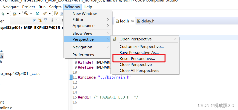
1、复位视图

使用的时候经常需要变化调试进入调试模式,因此这里可能就需要复位视图什么的,这里复位视图的方式都差不多,下图已给出:
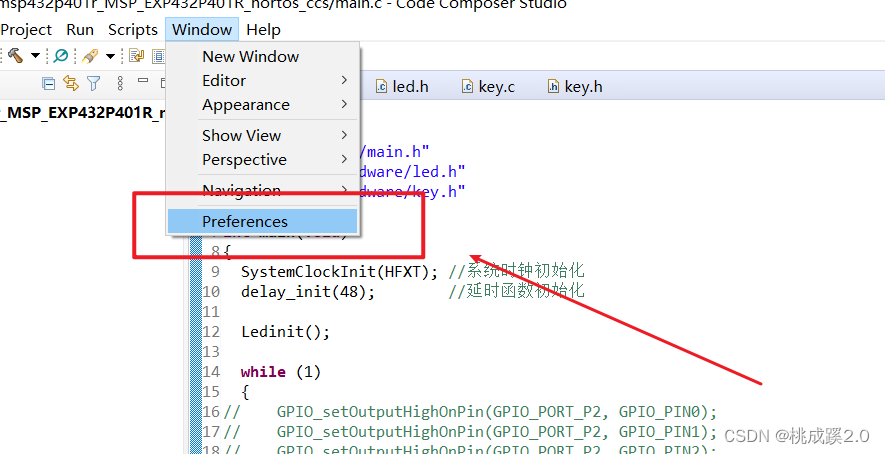
在这里插入图片描述

2、代码提示

这里还是跟cubeide很像的,都是套壳软件嘛,如下图所示进行点击可以进入查看
在这里插入图片描述
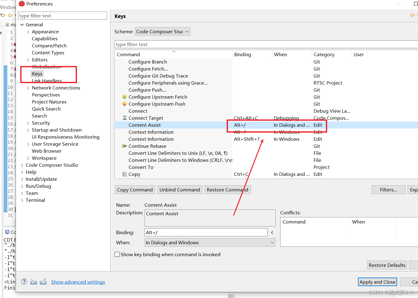
在这里可以看到代码提示的快捷键其实默认是ALT+/,这里可以根据自己的需求修改,如果想要实现自己进行修改,那就要自己去配置了,挺蛮烦的,有大佬配制好的现成的也行的其实。
在这里插入图片描述

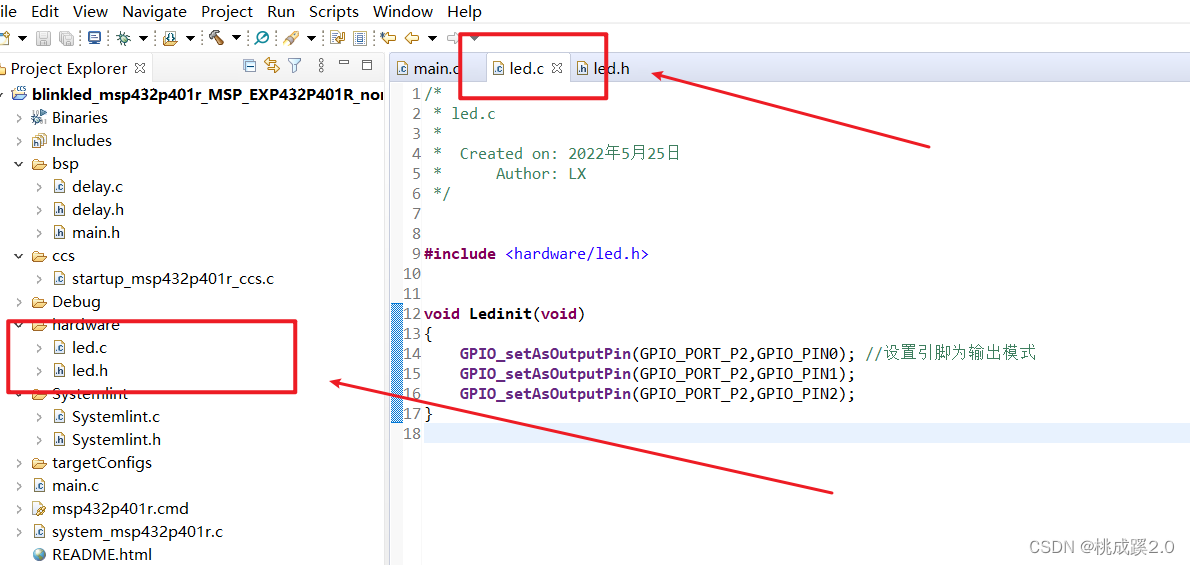
3、新建自己的硬件库(hardware)

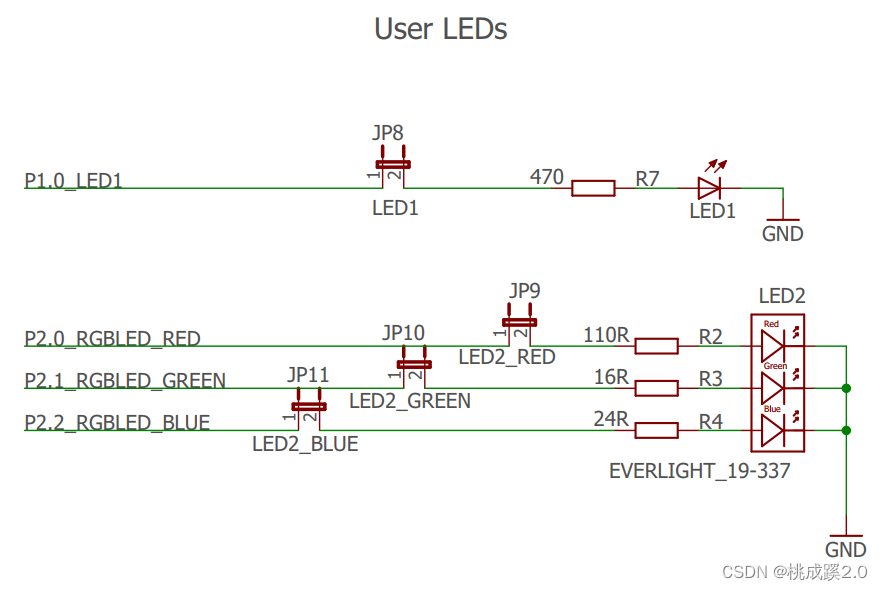
这里就是一些常见的外设,方便调用,就可以像正点原子一样写个hardware的样子了,下面是原理图部分的led部分,如下所示
在这里插入图片描述
下面是加入的库
在这里插入图片描述
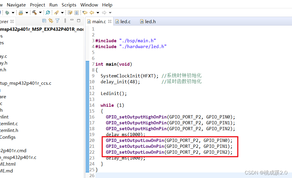
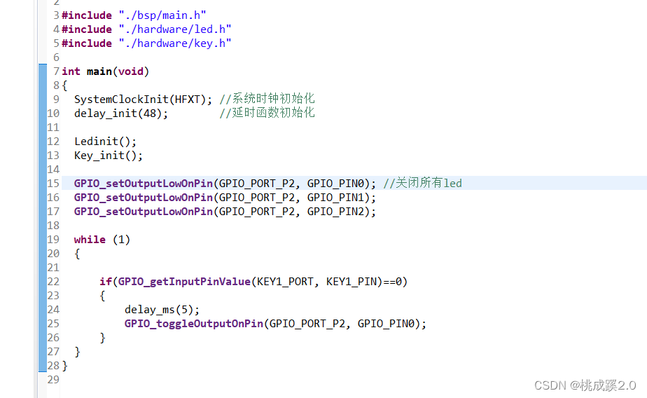
点灯操作如下即可了,先进行初始化,下面的就是进行高低电平配置了
在这里插入图片描述
下面来尝试按键部分,也是输入输出的口
在这里插入图片描述
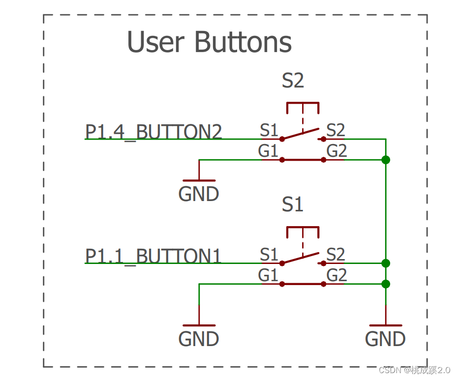
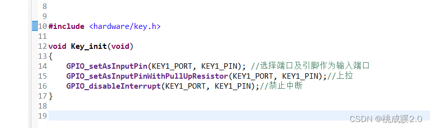
按键初始化,这里需要配置为输入模式,根据原理图的配置,配置为上拉输入,这样方便我们进行检测按键的输入
在这里插入图片描述
下面就是按键执行的函数了,如下所示,这样就可以实现按键控制led的变化了
在这里插入图片描述

4、中断的使用

添加中断初始化函数和使能,详情查看注释即可
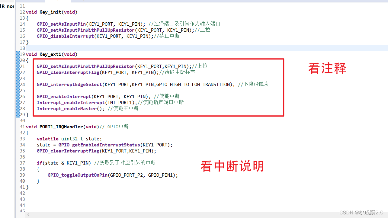
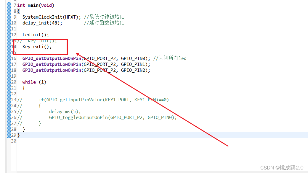
在这里插入图片描述
在主函数中加入按键初始化
在这里插入图片描述
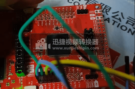
最终效果如下所示,可以看到按键改变led的执行效果。
在这里插入图片描述

MSP432 低功耗高性能并存10.1 Digital I/O Introduction The digital I/O features include: • Independently programmable individual I/Os • Any combination of input or output • Individually configurable interrupts for ports (available for certain ports only) • Independent input and output data registers • Individually configurable pullup or pulldown resistors • Wake-up capability from ultra-low power modes (available for certain ports only) • Individually configurable high drive I/Os (available for certain I/Os only) Devices within the family may have up to eleven digital I/O ports implemented (P1 to P10 and PJ). Most ports contain eight I/O lines; however, some ports may contain less (see the device-specific data sheet for ports available). Each I/O line is individually configurable for input or output direction, and each can be individually read or written. Each I/O line is individually configurable for pullup or pulldown resistors. Certain ports have interrupt and wake-up capability from ultra-low power modes (see device specific data sheet for ports with interrupt and wake-up capability). Each interrupt can be individually enabled and configured to provide an interrupt on a rising or falling edge of an input signal. All interrupts are fed into an encoded Interrupt Vector register, allowing the application to determine which sub-pin of a port has generated the event. Individual ports can be accessed as byte-wide ports or can be combined into half-word-wide ports. Port pairs P1 and P2, P3 and P4, P5 and P6, P7 and P8, and so on, are associated with the names PA, PB, PC, PD, and so on, respectively. All port registers are handled in this manner with this naming convention. The main exception are the interrupt vector registers, for example, interrupts for ports P1 and P2 must be handled through P1IV and P2IV, PAIV does not exist. When writing to port PA with half-word operations, all 16 bits are written to the port. When writing to the lower byte of port PA using byte operations, the upper byte remains unchanged. Similarly, writing to the upper byte of port PA using byte instructions leaves the lower byte unchanged. When writing to a port that contains less than the maximum number of bits possible, the unused bits are don't care. Ports PB, PC, PD, PE, and PF behave similarly.
评论
添加红包

请填写红包祝福语或标题

红包个数最小为10个

红包金额最低5元

当前余额3.43前往充值 >
需支付:10.00
成就一亿技术人!
领取后你会自动成为博主和红包主的粉丝 规则
hope_wisdom
发出的红包

打赏作者

桃成蹊2.0

你的鼓励将是我创作的最大动力

¥1 ¥2 ¥4 ¥6 ¥10 ¥20
扫码支付:¥1
获取中
扫码支付

您的余额不足,请更换扫码支付或充值

打赏作者

实付
使用余额支付
点击重新获取
扫码支付
钱包余额 0

抵扣说明:

1.余额是钱包充值的虚拟货币,按照1:1的比例进行支付金额的抵扣。
2.余额无法直接购买下载,可以购买VIP、付费专栏及课程。

余额充值