


xilinx vivado axi_quad_spi IP核四线转三线SPI读写ADI ADC FPGA实现(附源码)
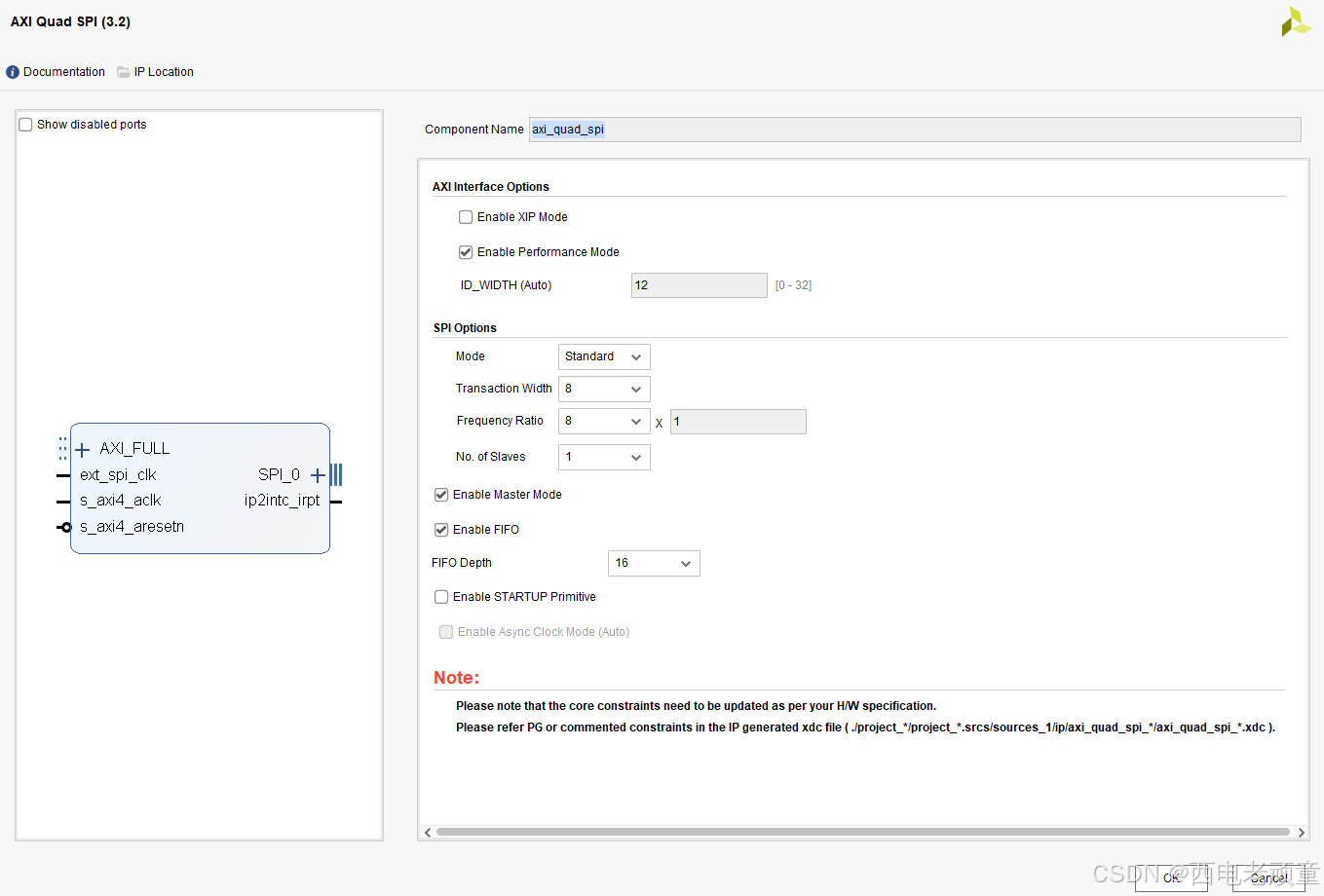
近期项目中,用到了xilinx axi_quad_spi模块,想通过该模块读写ADI公司的ADC,vivado中对应的IP核的配置参数如下
对应的FPGA读写配置代码如下:
//////////////////////////////////////////////////////////////////////////////////
// Company:  SYCP
// Engineer: 西电老顽童
//
// Create Date: 2024/10/10 14:38:02
// Design Name:
// Module Name: axi_quad_spi_test
// Project Name:
// Target Devices:
// Tool Versions:
// Description:
//     This interface is used to connect Xilinx axi_quad_spi IP and ADI 3 wire-spi devices,the SPI transfer payload is  [ W/R   Addr    DATA]
// Dependencies:
//
// Revision:
// Revision 0.01 - File Created
// Additional Comments:
//
//////////////////////////////////////////////////////////////////////////////////

module adi_axi_spi_interface#(
    parameter CLK_DIV    = 8'd4,  // ext_spi_clk/AXI_SPI_sck_o, correspond value is 2, 4, 8,....
    parameter ADDR_WIDTH = 8'd15,
    parameter DATA_WIDTH = 8'd8
)(

input   ext_spi_clk,   // connect to axi_quad_spi ext_spi_clk(at leset 2 times faster than AXI_SPI_sck_o)

input   AXI_SPI_sck_o, // connect to axi_quad_spi AXI_SPI_sck_o
inout   ad_sdio,       // connect to ADC spi sdio
output  ad_cs,         // connect to ADC spi cs
output  ad_spi_clk,

output  AXI_SPI_io0_i, // connect to axi_quad_spi AXI_SPI_io0_i
input   AXI_SPI_io0_o, // connect to axi_quad_spi AXI_SPI_io0_o(MOSI output)
input   AXI_SPI_io0_t, // connect to axi_quad_spi AXI_SPI_io0_t(low active)

output  AXI_SPI_io1_i, // connect to axi_quad_spi AXI_SPI_io1_i(MOSI input)
input   AXI_SPI_io1_o, // connect to axi_quad_spi AXI_SPI_io1_o
input   AXI_SPI_io1_t  // connect to axi_quad_spi AXI_SPI_io1_t
);


reg [2:0] AXI_SPI_sck_o_dly;
always @(posedge ext_spi_clk) begin
    AXI_SPI_sck_o_dly <= {AXI_SPI_sck_o_dly, AXI_SPI_sck_o};
end


reg [7:0] cnt, delay_cnt;
reg wr_flag;
localparam  IDLE     = 2'b00,
            TransCMD   = 2'b01,
            TransDATA  = 2'b10;
reg [1:0] STATE;
always @(posedge ext_spi_clk) begin
    if(AXI_SPI_io0_t)begin
	    cnt <= 0;
	    delay_cnt <= 0;
		wr_flag <= 0;
		STATE <= IDLE;
	end else begin
	     case(STATE)
            IDLE:begin
                if({AXI_SPI_sck_o_dly[0], AXI_SPI_sck_o} == 2'd1)begin
				    cnt <= cnt + 1'd1;
				    if(AXI_SPI_io0_o == 1'd0)begin // 1:write    0:read
					    wr_flag <= 1;
					end
					STATE <= TransCMD;
                end
                else begin
				    cnt <= 0;
				    delay_cnt <= 0;
					wr_flag <= 0;
                    STATE <= IDLE;
                end
            end

			TransCMD:begin
			    if({AXI_SPI_sck_o_dly[0], AXI_SPI_sck_o} == 2'd1)begin // rising edge
				    cnt <= cnt + 1'd1;
					if(cnt <= ADDR_WIDTH - 1)begin
					    STATE <= TransCMD;
					end else begin
					    delay_cnt <= delay_cnt + 1'd1;
					    STATE <= TransDATA;
					end
				end
			end

			TransDATA:begin
			    delay_cnt <= 0;
			    if({AXI_SPI_sck_o_dly[0], AXI_SPI_sck_o} == 2'd1)begin // rising edge
			        cnt <= cnt + 1'd1;
			        if(cnt <= ADDR_WIDTH -1 + DATA_WIDTH)begin
					    STATE <= TransDATA;
					end else begin
					    STATE <= IDLE;
					end
			    end
			end

            default:STATE <= IDLE;
        endcase

    end
end


assign ad_sdio    =  (cnt <= ADDR_WIDTH) ? AXI_SPI_io0_o
                                         : wr_flag ? AXI_SPI_io0_o
                                                   : 1'dz;
assign ad_cs      = AXI_SPI_io0_t;
assign ad_spi_clk = AXI_SPI_sck_o;
assign AXI_SPI_io1_i = ad_sdio;

endmodule
上面代码已经在项目中使用两个月了,运行可靠。
需要注意的一点就是,axi时钟要分频后(一般4倍或以上)来配置IP核。
另外,spi总线payload我们使用的是24bit模式。如果想用其它模式payload,自行修改吧。
祝好运!


 4689
4689

 被折叠的 条评论
为什么被折叠?
被折叠的 条评论
为什么被折叠?
 到【灌水乐园】发言


