


 本文记录基于AXI4-Lite协议实现PS与PL区交互的实验。通过PS向PL发送指令控制LED呼吸灯频率,PL检测按键返回数据。实验分三部分,在Vivado用Verilog搭建Soc系统工程,在Vitis用C语言搭建SDK工程,最终PS读取PL数据、写入数据均成功。
最近在学axi4-lite协议,就简单记录一下。
实验概述:通过AXI-Lite实现PS与PL区之间的简单读写功能,其中PS端作为主机,PL端作为从机。PS向PL发送控制指令,以控制PS区LED呼吸灯的频率,实现写操作;PL端检测按键Key的情况,根据按键情况将不同的数据返回给PS端,实现读操作。(原本实验的读操作是读一个温度传感器的数据,但我这边没有器件就改更简单的按键了)
软件环境:Vivado 2020.1
硬件环境:Zynq UltraScale + MPSoC XCZU3EG
实验主要分三部分:分别对应在Vivado软件上使用Verilog编程搭建Soc系统工程(FPGA开发)、在Vitis平台使用C语言搭建SDK工程(ARM)以及实验结果。
1、搭建Soc系统工程
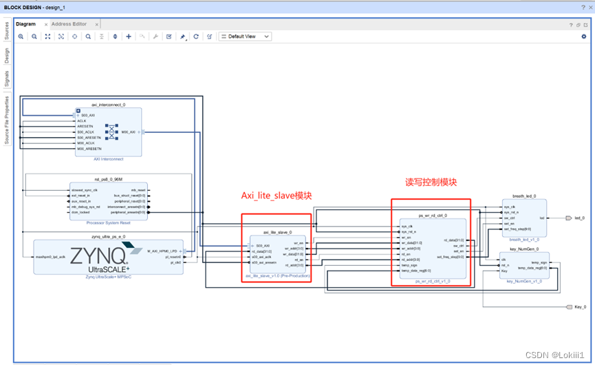 其中,axi_lite_slave和ps_wr_rd_ctrl模块是核心模块。axi_lite_slave是在官方IP代码基础上进行修改的,ps_wr_rd_ctrl模块是自己写的,用于解析指令,产生读写操作的信号。
(1)Axi_lite_slave
Axi_lite从机模块,主要是基于官方IP代码稍作修改(修改不多)
`timescale 1 ns / 1 ps

	module axi_lite_slave_v1_0_S00_AXI #
	(
		// Users to add parameters here

		// User parameters ends
		// Do not modify the parameters beyond this line

		// Width of S_AXI data bus
		parameter integer C_S_AXI_DATA_WIDTH	= 32,
		// Width of S_AXI address bus
		parameter integer C_S_AXI_ADDR_WIDTH	= 4
	)
	(
		// Users to add ports here
		output wr_en,	//写使能,高表示写数据、写地址有效
		output [3:0] wr_addr,	//写数据(PS->PL)
		output [31:0] wr_data,	//写地址(PS->PL)
		output rd_en,	//读使能,高表示读数据、读地址有效
		output [3:0] rd_addr,	//读地址(PL->PS)

		input [31:0] rd_data,	//读数据(PL->PS)

		// User ports ends
		// Do not modify the ports beyond this line

		// Global Clock Signal
		input wire  S_AXI_ACLK,
		// Global Reset Signal. This Signal is Active LOW
		input wire  S_AXI_ARESETN,
		// Write address (issued by master, acceped by Slave)
		input wire [C_S_AXI_ADDR_WIDTH-1 : 0] S_AXI_AWADDR,
		// Write channel Protection type. This signal indicates the
    		// privilege and security level of the transaction, and whether
    		// the transaction is a data access or an instruction access.
		input wire [2 : 0] S_AXI_AWPROT,
		// Write address valid. This signal indicates that the master signaling
    		// valid write address and control information.
		input wire  S_AXI_AWVALID,
		// Write address ready. This signal indicates that the slave is ready
    		// to accept an address and associated control signals.
		output wire  S_AXI_AWREADY,
		// Write data (issued by master, acceped by Slave)
		input wire [C_S_AXI_DATA_WIDTH-1 : 0] S_AXI_WDATA,
		// Write strobes. This signal indicates which byte lanes hold
    		// valid data. There is one write strobe bit for each eight
    		// bits of the write data bus.
		input wire [(C_S_AXI_DATA_WIDTH/8)-1 : 0] S_AXI_WSTRB,
		// Write valid. This signal indicates that valid write
    		// data and strobes are available.
		input wire  S_AXI_WVALID,
		// Write ready. This signal indicates that the slave
    		// can accept the write data.
		output wire  S_AXI_WREADY,
		// Write response. This signal indicates the status
    		// of the write transaction.
		output wire [1 : 0] S_AXI_BRESP,
		// Write response valid. This signal indicates that the channel
    		// is signaling a valid write response.
		output wire  S_AXI_BVALID,
		// Response ready. This signal indicates that the master
    		// can accept a write response.
		input wire  S_AXI_BREADY,
		// Read address (issued by master, acceped by Slave)
		input wire [C_S_AXI_ADDR_WIDTH-1 : 0] S_AXI_ARADDR,
		// Protection type. This signal indicates the privilege
    		// and security level of the transaction, and whether the
    		// transaction is a data access or an instruction access.
		input wire [2 : 0] S_AXI_ARPROT,
		// Read address valid. This signal indicates that the channel
    		// is signaling valid read address and control information.
		input wire  S_AXI_ARVALID,
		// Read address ready. This signal indicates that the slave is
    		// ready to accept an address and associated control signals.
		output wire  S_AXI_ARREADY,
		// Read data (issued by slave)
		output wire [C_S_AXI_DATA_WIDTH-1 : 0] S_AXI_RDATA,
		// Read response. This signal indicates the status of the
    		// read transfer.
		output wire [1 : 0] S_AXI_RRESP,
		// Read valid. This signal indicates that the channel is
    		// signaling the required read data.
		output wire  S_AXI_RVALID,
		// Read ready. This signal indicates that the master can
    		// accept the read data and response information.
		input wire  S_AXI_RREADY
	);

	// AXI4LITE signals
	reg [C_S_AXI_ADDR_WIDTH-1 : 0] 	axi_awaddr;
	reg  	axi_awready;
	reg  	axi_wready;
	reg [1 : 0] 	axi_bresp;
	reg  	axi_bvalid;
	reg [C_S_AXI_ADDR_WIDTH-1 : 0] 	axi_araddr;
	reg  	axi_arready;
	reg [C_S_AXI_DATA_WIDTH-1 : 0] 	axi_rdata;
	reg [1 : 0] 	axi_rresp;
	reg  	axi_rvalid;

	// Example-specific design signals
	// local parameter for addressing 32 bit / 64 bit C_S_AXI_DATA_WIDTH
	// ADDR_LSB is used for addressing 32/64 bit registers/memories
	// ADDR_LSB = 2 for 32 bits (n downto 2)
	// ADDR_LSB = 3 for 64 bits (n downto 3)
	localparam integer ADDR_LSB = (C_S_AXI_DATA_WIDTH/32) + 1;
	localparam integer OPT_MEM_ADDR_BITS = 1;
	//----------------------------------------------
	//-- Signals for user logic register space example
	//------------------------------------------------
	//-- Number of Slave Registers 4
	reg [C_S_AXI_DATA_WIDTH-1:0]	slv_reg0;
	reg [C_S_AXI_DATA_WIDTH-1:0]	slv_reg1;
	reg [C_S_AXI_DATA_WIDTH-1:0]	slv_reg2;
	reg [C_S_AXI_DATA_WIDTH-1:0]	slv_reg3;
	wire	 slv_reg_rden;
	wire	 slv_reg_wren;
	reg [C_S_AXI_DATA_WIDTH-1:0]	 reg_data_out;
	integer	 byte_index;
	reg	 aw_en;

	// I/O Connections assignments

	assign S_AXI_AWREADY	= axi_awready;
	assign S_AXI_WREADY	= axi_wready;
	assign S_AXI_BRESP	= axi_bresp;
	assign S_AXI_BVALID	= axi_bvalid;
	assign S_AXI_ARREADY	= axi_arready;
	assign S_AXI_RDATA	= axi_rdata;
	assign S_AXI_RRESP	= axi_rresp;
	assign S_AXI_RVALID	= axi_rvalid;
	// Implement axi_awready generation
	// axi_awready is asserted for one S_AXI_ACLK clock cycle when both
	// S_AXI_AWVALID and S_AXI_WVALID are asserted. axi_awready is
	// de-asserted when reset is low.

	always @( posedge S_AXI_ACLK )
	begin
	  if ( S_AXI_ARESETN == 1'b0 )
	    begin
	      axi_awready <= 1'b0;
	      aw_en <= 1'b1;
	    end
	  else
	    begin
	      if (~axi_awready && S_AXI_AWVALID && S_AXI_WVALID && aw_en)
	        begin
	          // slave is ready to accept write address when
	          // there is a valid write address and write data
	          // on the write address and data bus. This design
	          // expects no outstanding transactions.
	          axi_awready <= 1'b1;
	          aw_en <= 1'b0;
	        end
	        else if (S_AXI_BREADY && axi_bvalid)
	            begin
	              aw_en <= 1'b1;
	              axi_awready <= 1'b0;
	            end
	      else
	        begin
	          axi_awready <= 1'b0;
	        end
	    end
	end

	// Implement axi_awaddr latching
	// This process is used to latch the address when both
	// S_AXI_AWVALID and S_AXI_WVALID are valid.

	always @( posedge S_AXI_ACLK )
	begin
	  if ( S_AXI_ARESETN == 1'b0 )
	    begin
	      axi_awaddr <= 0;
	    end
	  else
	    begin
	      if (~axi_awready && S_AXI_AWVALID && S_AXI_WVALID && aw_en)
	        begin
	          // Write Address latching
	          axi_awaddr <= S_AXI_AWADDR;
	        end
	    end
	end

	// Implement axi_wready generation
	// axi_wready is asserted for one S_AXI_ACLK clock cycle when both
	// S_AXI_AWVALID and S_AXI_WVALID are asserted. axi_wready is
	// de-asserted when reset is low.

	always @( posedge S_AXI_ACLK )
	begin
	  if ( S_AXI_ARESETN == 1'b0 )
	    begin
	      axi_wready <= 1'b0;
	    end
	  else
	    begin
	      if (~axi_wready && S_AXI_WVALID && S_AXI_AWVALID && aw_en )
	        begin
	          // slave is ready to accept write data when
	          // there is a valid write address and write data
	          // on the write address and data bus. This design
	          // expects no outstanding transactions.
	          axi_wready <= 1'b1;
	        end
	      else
	        begin
	          axi_wready <= 1'b0;
	        end
	    end
	end

	// Implement memory mapped register select and write logic generation
	// The write data is accepted and written to memory mapped registers when
	// axi_awready, S_AXI_WVALID, axi_wready and S_AXI_WVALID are asserted. Write strobes are used to
	// select byte enables of slave registers while writing.
	// These registers are cleared when reset (active low) is applied.
	// Slave register write enable is asserted when valid address and data are available
	// and the slave is ready to accept the write address and write data.
	assign slv_reg_wren = axi_wready && S_AXI_WVALID && axi_awready && S_AXI_AWVALID;

	/*always @( posedge S_AXI_ACLK )
	begin
	  if ( S_AXI_ARESETN == 1'b0 )
	    begin
	      slv_reg0 <= 0;
	      slv_reg1 <= 0;
	      slv_reg2 <= 0;
	      slv_reg3 <= 0;
	    end
	  else begin
	    if (slv_reg_wren)
	      begin
	        case ( axi_awaddr[ADDR_LSB+OPT_MEM_ADDR_BITS:ADDR_LSB] )
	          2'h0:
	            for ( byte_index = 0; byte_index <= (C_S_AXI_DATA_WIDTH/8)-1; byte_index = byte_index+1 )
	              if ( S_AXI_WSTRB[byte_index] == 1 ) begin
	                // Respective byte enables are asserted as per write strobes
	                // Slave register 0
	                slv_reg0[(byte_index*8) +: 8] <= S_AXI_WDATA[(byte_index*8) +: 8];
	              end
	          2'h1:
	            for ( byte_index = 0; byte_index <= (C_S_AXI_DATA_WIDTH/8)-1; byte_index = byte_index+1 )
	              if ( S_AXI_WSTRB[byte_index] == 1 ) begin
	                // Respective byte enables are asserted as per write strobes
	                // Slave register 1
	                slv_reg1[(byte_index*8) +: 8] <= S_AXI_WDATA[(byte_index*8) +: 8];
	              end
	          2'h2:
	            for ( byte_index = 0; byte_index <= (C_S_AXI_DATA_WIDTH/8)-1; byte_index = byte_index+1 )
	              if ( S_AXI_WSTRB[byte_index] == 1 ) begin
	                // Respective byte enables are asserted as per write strobes
	                // Slave register 2
	                slv_reg2[(byte_index*8) +: 8] <= S_AXI_WDATA[(byte_index*8) +: 8];
	              end
	          2'h3:
	            for ( byte_index = 0; byte_index <= (C_S_AXI_DATA_WIDTH/8)-1; byte_index = byte_index+1 )
	              if ( S_AXI_WSTRB[byte_index] == 1 ) begin
	                // Respective byte enables are asserted as per write strobes
	                // Slave register 3
	                slv_reg3[(byte_index*8) +: 8] <= S_AXI_WDATA[(byte_index*8) +: 8];
	              end
	          default : begin
	                      slv_reg0 <= slv_reg0;
	                      slv_reg1 <= slv_reg1;
	                      slv_reg2 <= slv_reg2;
	                      slv_reg3 <= slv_reg3;
	                    end
	        endcase
	      end
	  end
	end    */

	// Implement write response logic generation
	// The write response and response valid signals are asserted by the slave
	// when axi_wready, S_AXI_WVALID, axi_wready and S_AXI_WVALID are asserted.
	// This marks the acceptance of address and indicates the status of
	// write transaction.

	always @( posedge S_AXI_ACLK )
	begin
	  if ( S_AXI_ARESETN == 1'b0 )
	    begin
	      axi_bvalid  <= 0;
	      axi_bresp   <= 2'b0;
	    end
	  else
	    begin
	      if (axi_awready && S_AXI_AWVALID && ~axi_bvalid && axi_wready && S_AXI_WVALID)
	        begin
	          // indicates a valid write response is available
	          axi_bvalid <= 1'b1;
	          axi_bresp  <= 2'b0; // 'OKAY' response
	        end                   // work error responses in future
	      else
	        begin
	          if (S_AXI_BREADY && axi_bvalid)
	            //check if bready is asserted while bvalid is high)
	            //(there is a possibility that bready is always asserted high)
	            begin
	              axi_bvalid <= 1'b0;
	            end
	        end
	    end
	end

	// Implement axi_arready generation
	// axi_arready is asserted for one S_AXI_ACLK clock cycle when
	// S_AXI_ARVALID is asserted. axi_awready is
	// de-asserted when reset (active low) is asserted.
	// The read address is also latched when S_AXI_ARVALID is
	// asserted. axi_araddr is reset to zero on reset assertion.

	always @( posedge S_AXI_ACLK )
	begin
	  if ( S_AXI_ARESETN == 1'b0 )
	    begin
	      axi_arready <= 1'b0;
	      axi_araddr  <= 32'b0;
	    end
	  else
	    begin
	      if (~axi_arready && S_AXI_ARVALID)
	        begin
	          // indicates that the slave has acceped the valid read address
	          axi_arready <= 1'b1;
	          // Read address latching
	          axi_araddr  <= S_AXI_ARADDR;
	        end
	      else
	        begin
	          axi_arready <= 1'b0;
	        end
	    end
	end

	// Implement axi_arvalid generation
	// axi_rvalid is asserted for one S_AXI_ACLK clock cycle when both
	// S_AXI_ARVALID and axi_arready are asserted. The slave registers
	// data are available on the axi_rdata bus at this instance. The
	// assertion of axi_rvalid marks the validity of read data on the
	// bus and axi_rresp indicates the status of read transaction.axi_rvalid
	// is deasserted on reset (active low). axi_rresp and axi_rdata are
	// cleared to zero on reset (active low).
	always @( posedge S_AXI_ACLK )
	begin
	  if ( S_AXI_ARESETN == 1'b0 )
	    begin
	      axi_rvalid <= 0;
	      axi_rresp  <= 0;
	    end
	  else
	    begin
	      if (axi_arready && S_AXI_ARVALID && ~axi_rvalid)
	        begin
	          // Valid read data is available at the read data bus
	          axi_rvalid <= 1'b1;
	          axi_rresp  <= 2'b0; // 'OKAY' response
	        end
	      else if (axi_rvalid && S_AXI_RREADY)
	        begin
	          // Read data is accepted by the master
	          axi_rvalid <= 1'b0;
	        end
	    end
	end

	// Implement memory mapped register select and read logic generation
	// Slave register read enable is asserted when valid address is available
	// and the slave is ready to accept the read address.
	assign slv_reg_rden = axi_arready & S_AXI_ARVALID & ~axi_rvalid;
	/*always @(*)
	begin
	      // Address decoding for reading registers
	      case ( axi_araddr[ADDR_LSB+OPT_MEM_ADDR_BITS:ADDR_LSB] )
	        2'h0   : reg_data_out <= slv_reg0;
	        2'h1   : reg_data_out <= slv_reg1;
	        2'h2   : reg_data_out <= slv_reg2;
	        2'h3   : reg_data_out <= slv_reg3;
	        default : reg_data_out <= 0;
	      endcase
	end

	// Output register or memory read data
	always @( posedge S_AXI_ACLK )
	begin
	  if ( S_AXI_ARESETN == 1'b0 )
	    begin
	      axi_rdata  <= 0;
	    end
	  else
	    begin
	      // When there is a valid read address (S_AXI_ARVALID) with
	      // acceptance of read address by the slave (axi_arready),
	      // output the read dada
	      if (slv_reg_rden)
	        begin
	          axi_rdata <= reg_data_out;     // register read data
	        end
	    end
	end    */

	// Add user logic here

	assign wr_en = slv_reg_wren;
	assign wr_addr = axi_awaddr;
	assign wr_data = S_AXI_WDATA;
	assign rd_en = slv_reg_rden;
	assign rd_addr = axi_araddr;
	assign S_AXI_RDATA = rd_data;
	// User logic ends

	endmodule
然后是顶层模块,记得例化也要加上 新定义的信号。
(2)ps_wr_rd_ctrl
module ps_wr_rd_ctrl(
		input				sys_clk,
		input				sys_rst_n,

	    // connect to module"axi_lite_slave"
		input				wr_en,
		input	    [31:0]	wr_data,
		input	    [3:0]	wr_addr,
		input				rd_en,
		input	    [3:0]	rd_addr,
		output reg	[31:0]	rd_data,

		input				temp_sign,
		input		[6:0]   temp_data_reg,
		output              sw_ctrl,
        output              set_en,
        output   [9:0]      set_freq_step

	);

reg			sw_ctrl_reg;
reg	[31:0]	set_en_and_step_reg;

assign sw_ctrl = sw_ctrl_reg;
assign set_en  = set_en_and_step_reg[0];
assign set_freq_step = set_en_and_step_reg[17:8];

// receive data form ps
always @(posedge sys_clk or negedge sys_rst_n) begin
	if (!sys_rst_n) begin
		sw_ctrl_reg <= 1'b0;
		set_en_and_step_reg <= 'd0;
	end
	else if (wr_en) begin
		case(wr_addr)
			0 : sw_ctrl_reg         <= wr_data[0];
			4 : set_en_and_step_reg <= wr_data;
			default : ;
		endcase
	end
	else begin
		sw_ctrl_reg <= sw_ctrl_reg;
		set_en_and_step_reg <= 'd0;
	end
end

// send data  to ps
always @(posedge sys_clk or negedge sys_rst_n) begin
	if (!sys_rst_n) begin
		rd_data <= 'd0;
	end
	else if (rd_en) begin
		case(rd_addr)
			0 : rd_data[0]   <= temp_sign;
			4 : rd_data[6:0] <= temp_data_reg;
			default : ;
		endcase
	end
	else begin
		rd_data <= 'd0;
	end
end

endmodule
(3)breath_led
module breath_led(
    input wire sys_clk,
    input wire sys_rst_n,
    input wire sw_ctrl, //呼吸灯开关控制信号,1亮 0灭
    input wire set_en,  //设置呼吸灯频率的设置使能信号,1设置有效 0无效
    input [9:0] set_freq_step,  //设置呼吸灯频率变化步长

    output wire led
    );

    parameter START_FREQ_STEP = 10'd100;  //设置频率步长初始值

    reg [15:0] period_cnt;  //周期计数器
    reg [15:0] duty_cycle;   //高电平占空比的计数器
    reg [9:0] freq_step;    //呼吸灯频率间隔步长
    reg inc_dec_flag;   //为1时表示占空比递减,为0时表示占空比递增

    wire led_t;
    assign led_t = (period_cnt <= duty_cycle) ? 1'b1 : 1'b0;
    assign led = led_t & sw_ctrl;

    //period_cnt:0-50_000
    always@(posedge sys_clk or negedge sys_rst_n) begin
        if((!sys_rst_n) || (!sw_ctrl))
            period_cnt <= 16'b0;
        else if(period_cnt == 16'd50_000)
            period_cnt <= 16'b0;
        else
            period_cnt <= period_cnt + 1'b1;
    end

    //设置频率间隔freq_step(0-1000),通过输入信号set_freq_step和set_en控制
    always@(posedge sys_clk or negedge sys_rst_n) begin
        if(!sys_rst_n)
            freq_step <= START_FREQ_STEP;
        else if(set_en) begin
            if(set_freq_step == 1'b0)
                freq_step <=10'd1;
            else begin
                if(set_freq_step >= 10'd1000)
                    freq_step <= 10'd1000;
                else
                    freq_step <= set_freq_step;
            end
        end
    end

    //调节高电平占空比的计数值duty_cycle
    always@(posedge sys_clk or negedge sys_rst_n) begin
        if((!sys_rst_n) || (!sw_ctrl)) begin
            duty_cycle <= 16'd0;
            inc_dec_flag <= 1'b0;
        end
        //每次计数完一个周期(0-50_000),就调节占空比计数值duty_cycle
        else if(period_cnt == 16'd50_000) begin
            if(inc_dec_flag) begin  //占空比递减
                if(duty_cycle == 16'd0)
                    inc_dec_flag <= 1'b0;
                else if(duty_cycle < freq_step)
                    duty_cycle <= 16'd0;
                else
                    duty_cycle <= duty_cycle - freq_step;
            end
            else begin  //占空比递增(也正是默认状态)
                if(duty_cycle >= 16'd50_000)
                    inc_dec_flag <= 1'b1;
                else
                    duty_cycle <= duty_cycle + freq_step;
            end
        end
        else   //duty_cycle未计完一个周期,占空比保持不变
            duty_cycle <= duty_cycle;
    end

endmodule
(4)key_NumGen
module key_NumGen(
input clk,
input rst_n,
input Key,
output reg temp_sign, //表示按下的状态
output reg [6:0] temp_data_reg //数据
);
always@(posedge clk or negedge rst_n) begin
if(!rst_n) begin
temp_sign <= 1'b0;
temp_data_reg <= 7'b0;
end
else begin
if(Key) begin //未按下
temp_sign <=1'b0;
temp_data_reg <= 7'b1111111;
end
else begin //按下
temp_sign <= 1'b1;
temp_data_reg <= 7'b1000001;
end
end
end
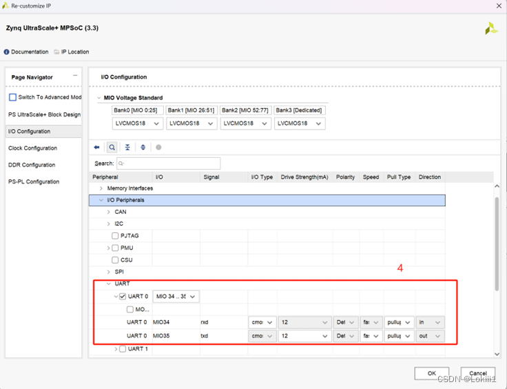
endmodule(5)ZYNQ_ultrascale+MPSoc
也就是PS端的ARM,进行的配置主要有:
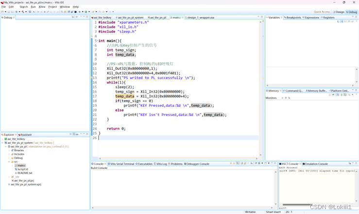
2、搭建Vitis-sdk工程
PS端的C语言实现比较容易,有一点需要注意的是使用Xil_In/Out函数时的地址要和Vivado里分配的地址相匹配。代码就简单贴出来:
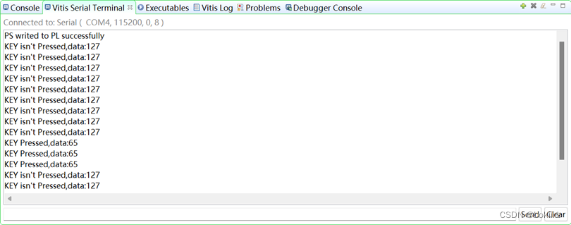
3、实验结果
打开串口终端,结果表明:当KEY没被按下时会收到data=127,当KEY被按下时data=65。PS读取PL数据成功。
此外,板子上的LED呼吸灯闪烁,说明PS向PL写入数据成功。(忘记拍照片了)
参考:FPGA:基于AXI4_Lite的PS与PL交互项目、[3-4]程序设计、ZYNQ PS与PL交互专题_哔哩哔哩_bilibili


 8795
8795

 被折叠的 条评论
为什么被折叠?
被折叠的 条评论
为什么被折叠?
 到【灌水乐园】发言


