 Verilog实现2-单端口同步读写SRAM


 本文介绍了如何用Verilog实现一个位宽8bit、深度16bit的单端口同步读写SRAM。通过定义参数实现位宽和深度的可调。文中详细阐述了原理,包括输入输出端口的功能,以及在不同信号控制下的读写操作。还展示了代码实现和仿真结果,指出了初始化和we信号切换时的问题,并提供了参考文献。
之前在Verilog实现RAM(1)中,对常见存储器件进行了名词扫盲,并通过调用IP核实现了简单的同步读写SRAM;现在接着之前的工作,对同步读写SRAM进行Verilog描述----实现一个位宽8bit,深度16bit的单端口SRAM;
一、原理
输入端口有:
reg [3:0]a;//输入地址(RAM深度为16,对应地址位宽为4)
reg clk;//时钟
reg we;// write enable,写使能时进行RAM写操作
同时添加如下端口:
reg oe;// output enable,输出使能时RAM读取的结果才能输出
reg cs;// 片选信号,选择读取哪一个RAM
输出输出端口有:
wire [7:0]d;//读取RAM时数据输出/写入RAM时数据输入
工作过程如下:
时钟来临时,根据cs/we/oe的值执行不同的操作;cs有效(为1)、we为1时,写使能,将d输入数据写入a对应地址处;cs有效(为1)、we为0时,读使能,oe有效(为1)时将a地址处的数据读出到d上;
二、代码实现
接着之前的工作,对同步读写SRAM进行Verilog描述----实现一个位宽8bit,深度16bit的单端口SRAM;为增加灵活性,通过parameter定义位宽以及深度,实现SRAM位宽、深度可调;使用parameter定义参数以及参数重写见Verilog中Parameter用法-常量定义与参数传递(例化传递、defparam传递),此处只关心RAM的实现;
Verilog实现代码:
`timescale 1ns / 1ps
//////////////////////////////////////////////////////////////////////////////////
// Company:
// Engineer: guoliang CLL
//
// Create Date: 2020/02/23 12:06:07
// Design Name:
// Module Name: sram_sp_srsw
// Project Name:
// Target Devices:
// Tool Versions:
// Description:
//
// Dependencies:
//
// Revision:
// Revision 0.01 - File Created
// Additional Comments:
//
//////////////////////////////////////////////////////////////////////////////////


module sram_sp_srsw
#(parameter DW = 8,AW = 4)
(
    input [AW-1:0]a,//address
    input clk,
    input cs,// chip select
    input oe,// output enable
    input we,// write enable
    inout [DW-1:0]d// data
    );

//
parameter DP = 1 << AW;// depth
reg [DW-1:0]mem[0:DP-1];
reg [DW-1:0]reg_d;
//
always@(posedge clk)
begin
    if(cs & we)//write declaration
        begin
            mem[a] <= d;
        end
    else if(cs & !we & oe)
        begin
            reg_d <= mem[a];
        end
    else
        begin
            mem[a] <= mem[a];
            reg_d <= reg_d;
        end
end
//
assign d = (cs & !we & oe) ? reg_d : {DW{1'bz}};
endmodule
测试文件:
`timescale 1ns / 1ps
//////////////////////////////////////////////////////////////////////////////////
// Company:
// Engineer: guoliang CLL
//
// Create Date: 2020/02/23 16:29:54
// Design Name:
// Module Name: sram_sp_srsw_tsb
// Project Name:
// Target Devices:
// Tool Versions:
// Description:
//
// Dependencies:
//
// Revision:
// Revision 0.01 - File Created
// Additional Comments:
//
//////////////////////////////////////////////////////////////////////////////////


module sram_sp_srsw_tsb(

    );
// port declaration
reg [3:0]a;//address
reg clk;
reg cs;
reg oe;
reg we;// write enable
wire [7:0]d;//datain/out
// reg declaration
reg [7:0]din;
//
initial
begin
    clk = 1'b0;
    forever #10 clk = ~clk;//period = 20
end
//
assign d = (cs & we)?din:8'bzzzz_zzzz;
//
initial
begin
    a = 4'b0000;
    din = 8'd1;
    we = 1'b0;
    oe = 1'b1;
    cs = 1'b1;
    #20//read
    repeat(15) #20 a = a+1'b1;
    #20//write
    we = 1'b1;
    repeat(15) begin
        #20 a = a-1'b1;
        din = din+1'b1;
    end
    #20//read
    we = 1'b0;
    repeat(15) begin
        #20 a = a+1'b1;
    end
end
// instantation
    sram_sp_srsw inst (
      .a(a),      // input wire [3 : 0] a
      .d(d),      // input wire [7 : 0] d
      .clk(clk),  // input wire clk
      .we(we),    // input wire we
      .cs(cs),
      .oe(oe)
    );
endmodule
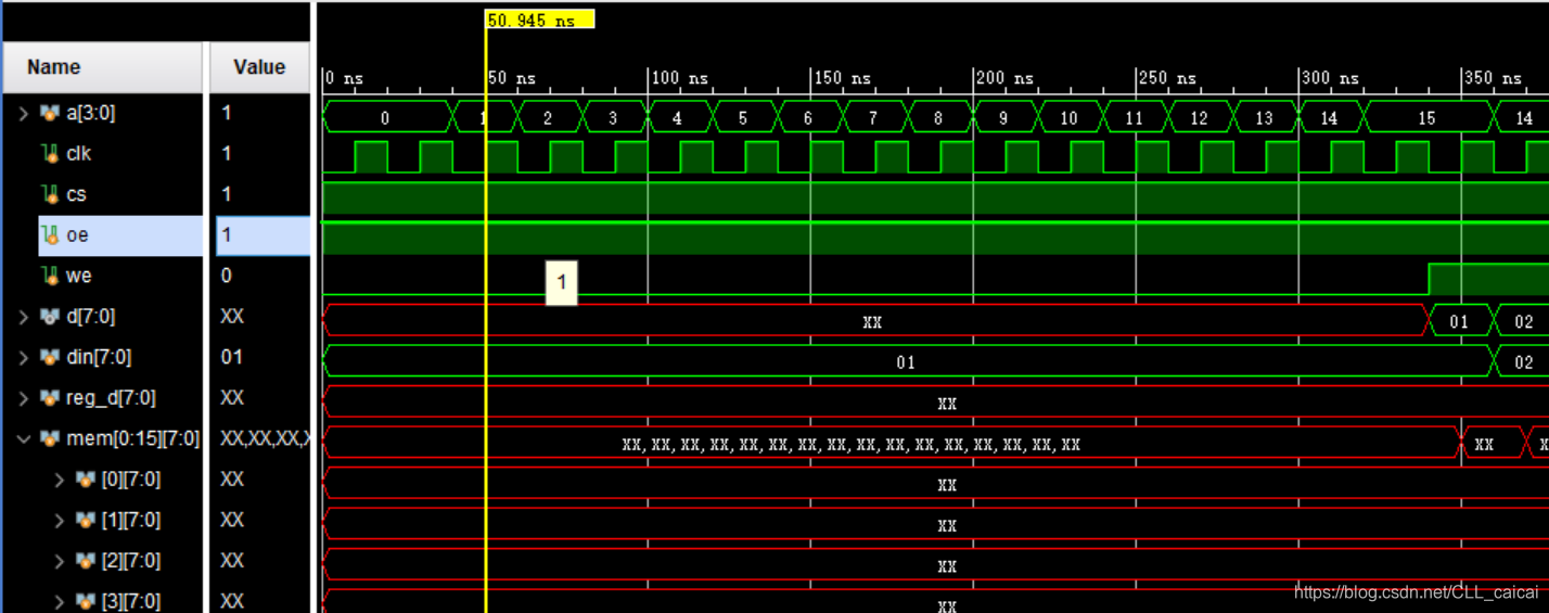
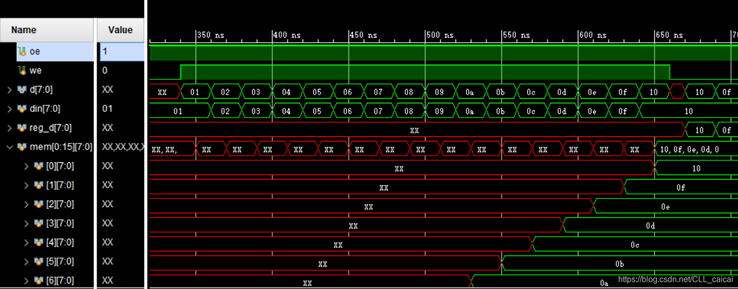
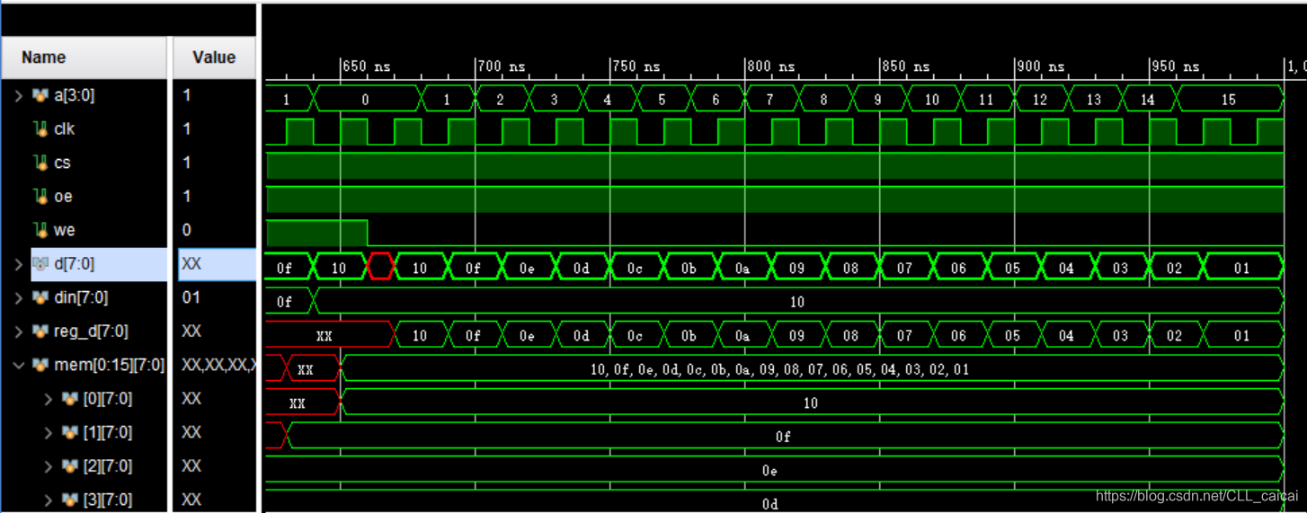
仿真结果:
首次读:
写:
再次读:
可以看出,因为没有初始化,直接读SARM时读出结果为不定值;
SRAM写时,存储空间被按照地址被逐个写入;
再次读时,读出刚刚写入的值;基础逻辑正确;
存在的问题:
1、如何初始化
2、we从1-0的瞬间,d存在不定态;如何解决仍待解决
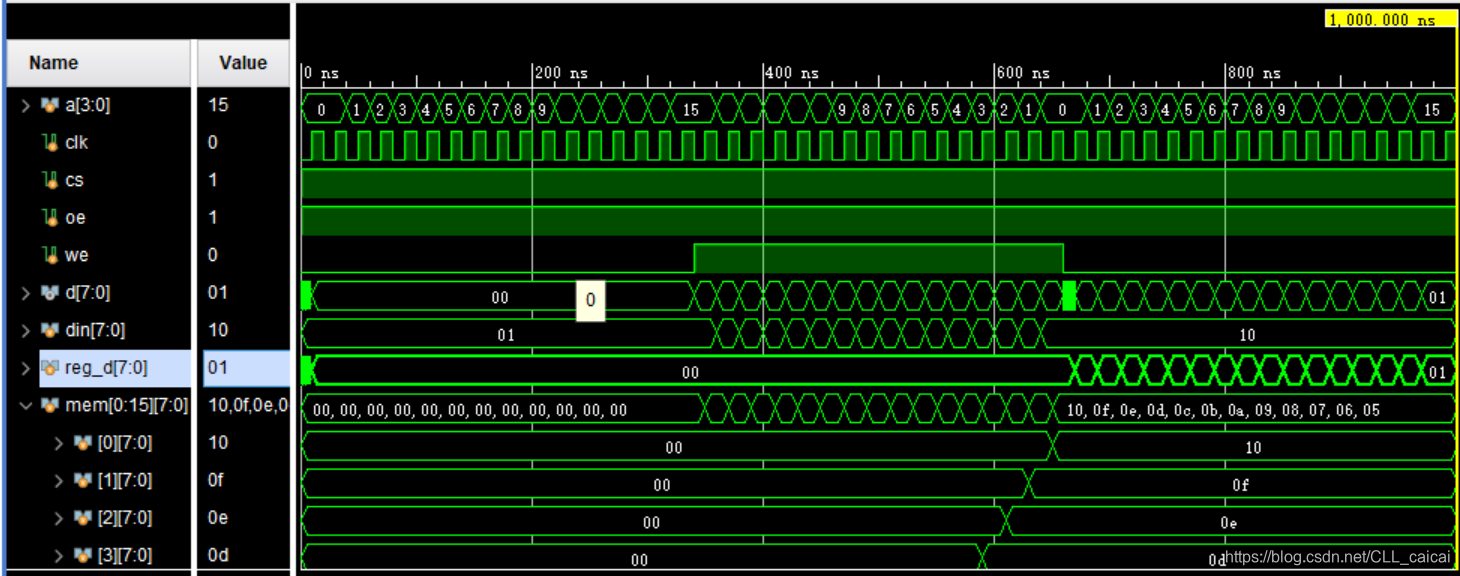
参考别人代码以后,将初始化部分复制过来:
//initialization
// synopsys_translate_off
integer i;
initial begin
    for(i=0; i < DP; i = i + 1) begin
        mem[i] = 8'h00;
    end
end
// synopsys_translate_on
随后进行仿真,确实初始化成功了;具体Verilog编译器指示语句的知识会在转载引导语句“// synopsys translate_off”中给出;
三、参考文献
https://baike.baidu.com/item/%E9%AB%98%E9%98%BB%E6%80%81/7062370?fr=aladdin


 7570
7570


 到【灌水乐园】发言


