


DA14580蓝牙硬件系统总览(三)
接续上一篇:DA14580蓝牙硬件系统总览(二)
3.7 TIMERS
3.7.1 Software timer
The Software timer block contains 2 timer modules that are software controlled, programmable and can be used for various tasks.
软件计时器块包含2个计时器模块,这些模块由软件控制,可编程,并且可以用于各种任务。
Timer 0 计时器0
• 16-bit general purpose timer
•16位通用定时器
• Ability to generate 2 Pulse Width Modulated signals (i.e. PWM0 and PWM1 but common programming)
•能够生成2个脉宽调制信号(即PWM0和PWM1,但通用编程)
• Programmable output frequency:
f = (16, 8, 4, 2 MHz or 32 kHz) / (M+1)+(N+1)
with N = 0 to (2^16)-1, M = 0 to (2 ^16)-1
•可编程输出频率:
f =(16、8、4、2 MHz或32 kHz)/(M + 1)+(N + 1)
其中N = 0至(2 ^16)-1,M = 0至(2 ^ 16)-1
• Programmable duty cycle:
•可编程占空比:

• Separately programmable interrupt timer:
•可单独编程的中断计时器:

Timer 2 计时器2
• 14-bit general purpose timer
• Ability to generate 3 Pulse Width Modulated signals (i.e. PWM2, PWM3 and PWM4)
• Input clock frequency: 16 MHz
• Programmable output frequency
F = 16 MHz/2 to 16 MHz/((2^14)-1)
• Three outputs with Programmable duty cycle from 0 % to 100 %
• Used for white LED intensity (on/off) control
•14位通用定时器
•能够生成3个脉宽调制信号(即PWM2,PWM3和PWM4)
•输入时钟频率:16 MHz
•可编程输出频率
F = 16 MHz / 2至16 MHz/(2 ^ 14)-1)
•三个输出,可编程占空比从0%到100%
•用于白光LED强度(开/关)控制
3.7.2 Wake-Up timer (唤醒定时器)
The Wake-up timer can be programmed to wake up the DA14580 from power down mode after a preprogrammed number of GPIO events.
可以对唤醒定时器进行编程,以在预编程数量的GPIO事件之后将DA14580从掉电模式唤醒。
Features 特色
• Monitors any GPIO state change
•监视任何GPIO状态更改
• Implements debouncing time from 0 upto 63 ms
•实现从0到63 ms的去抖动时间
• Accumulates external events and compares the number to a programmed value
•累积外部事件并将数字与编程值进行比较
• Generates an interrupt to the CPU
•产生中断给CPU
3.7.3 Watchdog timer(看门狗定时器)
The Watchdog timer is an 8-bit timer with sign bit that can be used to detect an unexpected execution sequence caused by a software run-away and can generate a full system reset or a Non-Maskable Interrupt (NMI).
看门狗定时器是一个带符号位的8位定时器,可用于检测由软件失控引起的意外执行序列,并可产生完整的系统复位或不可屏蔽中断(NMI)。
Features
• 8 bits down counter with sign bit, clocked with a 10.24 ms clock for a maximum 2.6 s time-out.
•8位带符号位的递减计数器,其时钟为10.24 ms,最大超时时间为2.6 s。
• Non-Maskable Interrupt (NMI) or WDOG reset.
•不可屏蔽中断(NMI)或WDOG复位。
• Optional automatic WDOG reset if NMI handler fails to update the Watchdog register.
•如果NMI处理程序无法更新看门狗寄存器,则可选的WDOG自动复位。
• Non-maskable Watchdog freeze of the Cortex-M0 Debug module when the Cortex-M0 is halted in Debug state.
•当Cortex-M0在调试状态下暂停时,Cortex-M0调试模块的不可屏蔽的看门狗冻结。
Maskable Watchdog freeze by user program. Note that if the system is not remapped, i.e. SysRAM is at address 0x20000000, then a watchdog fire will trigger the BootROM code to be executed again.
可屏蔽的看门狗被用户程序冻结。 请注意,如果未重新映射系统,即SysRAM位于地址0x20000000,则看门狗启动将触发BootROM代码再次执行。
3.8 CLOCK/RESET (时钟/复位)
3.8.1 Clocks 时钟
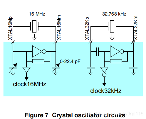
The Digital Controlled Xtal Oscillator (DXCO) is a Pierce configured type of oscillator designed for low power consumption and high stability. There are two such crystal oscillators in the system, one at 16MHz(XTAL16M) and a second at 32.768 kHz(XTAL32K). The 32.768 kHz oscillator has no trimming capabilities and is used as the clock of the Extended/Deep Sleep modes. The 16 MHz oscillator can be trimmed.
数字控制Xtal振荡器(DXCO)是Pierce配置的振荡器类型,设计用于低功耗和高稳定性。 系统中有两个这样的晶体振荡器,一个在16MHz(XTAL16M),另一个在32.768 kHz(XTAL32K)。 32.768 kHz振荡器没有修整功能,并用作扩展/深度睡眠模式的时钟。 16 MHz振荡器可以修整。
The principle schematic of the two oscillators is shown in Figure 7 below. No external components to the DA14580 are required other than the crystal itself. If the crystal has a case connection, it is advised to connect the case to ground.
两个振荡器的原理图如下图7所示。 除了晶体本身,DA14580不需要任何外部组件。 如果晶体与外壳连接,建议将外壳接地。
 There are 3 RC oscillators in the DA14580: one providing 16 MHz (RC16M), one providing 32 kHz (RC32K) and one providing a frequency in the range of 10.5 kHz(RCX).
DA14580中有3个RC振荡器:一个提供16 MHz(RC16M),一个提供32 kHz(RC32K),一个提供10.5 kHz(RCX)的频率。
3.8.2 Reset(重置、复位)
The DA14580 comprises an RST pad which is active high. It contains an RC filter for spikes suppression with 400 k and 2.8 pF for the resistor and the capacitor respectively. It also contains a 25 k pull-down resistor. This pad should be connected to ground if not needed by the application. The typical latency of the RST pad is in the range of 2 s.
DA14580包含一个高电平有效的RST焊盘。 它包含一个RC滤波器,用于抑制尖峰,电阻和电容器的峰值分别为400 k和2.8 pF。 它还包含一个25kΩ的下拉电阻。 如果应用程序不需要,则该焊盘应接地。 RST的典型等待时间在2 s的范围内,高电平有效。
3.9 POWER MANAGEMENT(电源管理)
The DA14580 has a complete power management function integrated with Buck or Boost DC-DC converter and separate LDOs for the different power domains of the system.
DA14580具有与Buck或Boost DC-DC转换器集成的完整电源管理功能,以及用于系统不同电源域的独立LDO。
Features 特色
• On-chip LDOs, without external capacitors
•片内LDO,无需外部电容器
• Synchronous DC-DC converter which can be configured as either:
•同步DC-DC转换器,可以将其配置为:
• Boost (step-up) converter, starting from 0.9 V, when running from an Alkaline/NiMH cell.
•使用碱性/ NiMH电池运行时,升压(升压)转换器从0.9 V开始。
• Buck (step-down) converter for increased efficiency when running from a Lithium coin-cell or 2 Alkaline batteries down to 2.2 V.
•Buck(降压)转换器可在使用锂纽扣电池或2节低至2.2 V的碱性电池供电时提高效率。
• On/Off control
•开/关控制
• Battery voltage measurement ADC (multiplexed input from general purpose ADC)
•电池电压测量ADC(通用ADC的复用输入)
• Use of small external components (2.2 uH inductor and 1uF capacitor)
•使用小型外部组件(2.2 uH电感器和1uF电容器)
The Power Block contains a DC-DC converter which can be configured to operate as a Step-Up or a Step Down converter. The converter provides power to four LDO groups in the system:
电源模块包含一个DC-DC转换器,可以将其配置为升压或降压转换器。 转换器为系统中的四个LDO组供电:
1. LDO RET: This is the LDO providing power to the Retention domain (PD_AON). It powers the Retention RAMs and the digital part which is always on.
LDO RET: 这是为保留域(PD_AON)提供电源的LDO。 它为保留RAM和始终打开的数字部分供电。
2. LDO OTP: This is the LDO powering the OTP macro cell. This is the reason for using the step-up DC-DC converter when running from an Alkaline battery.
LDO OTP: 这是为OTP宏单元供电的LDO。 这就是使用碱性电池供电时使用升压DC-DC转换器的原因。
3. LDO SYS: This is the LDO providing the system with the actual VDD power required for the digital part to operate. Note that the Power Block implements seamless switching from the LDO SYS to the LDO RET when the system enters Deep Sleep mode. In the latter case, a low voltage is applied to the PD_AON power domain to further reduce leakage.
LDO SYS: 这是为系统提供数字部分运行所需的实际VDD功率的LDO。 请注意,当系统进入深度睡眠模式时,电源块可实现从LDO SYS到LDO RET的无缝接缝切换。 在后一种情况下,将低电压施加到PD_AON电源域,以进一步减少泄漏。
4. LDO (various): This a group of LDOs used for the elaborate control of the powering up/down of the Radio, the GP ADC and the XTAL16M oscillator.
There are two ways of connecting external batteries to the Power Block of the DA14580. They depend on the specific battery cell used and its voltage range. Battery cells are distinguished into Lithium coin cells (2.2 V to 3.3 V) and Alkaline cells (1.0 V to 1.8 V). The connection diagrams are presented in Figure 9 and Figure 8 respectively:
LDO(各种): 这一组LDO用于精心控制无线电、GP ADC和XTAL16M振荡器的上电/掉电。
有两种方法可以将外部电池连接到DA14580的电源块。 它们取决于所使用的特定电池及其电压范围。 电池分为锂纽扣电池(2.2 V至3.3 V)和碱性电池(1.0 V至1.8 V)。 连接图分别如图9和图8所示:
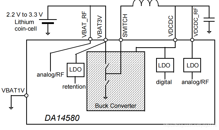 Figure 8 Supply overview, Coin-cell application 纽扣电池供电应用
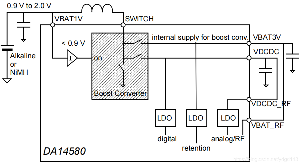 Figure 9 Supply overview, Alkaline-cell application 碱性电池供电应用
The usage of Boost or Buck mode with respect to the provided voltage ranges is illustrated in the following figure which also illustrates the efficiency of the engine assuming a 10 mA constant load.
下图说明了相对于提供的电压范围使用升压或降压模式的情况,该图还说明了假设10 mA恒定负载时工作的效率。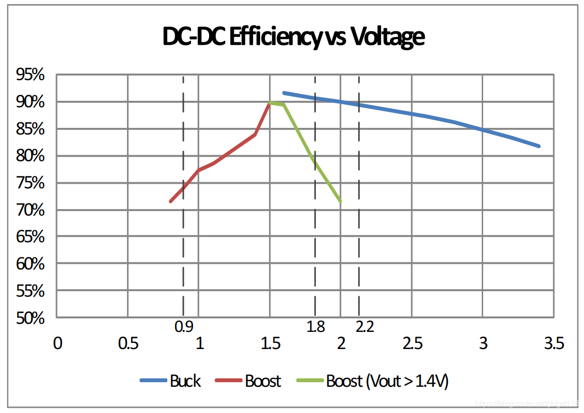 图10 各种电压时降压和升压模式的DC-DC效率对比
The X axis represents the supply voltage. BOOST mode should be used when voltage ranges from 0.9 V to 2.0 V to sustain a decent efficiency over 70 %. From that point on, the power dissipation becomes quite large.
X轴表示电源电压。当电压范围为0.9 V至2.0 V时,应使用BOOST模式,以保持70%以上的体面效率。从那时起,功率耗散变得相当大。
BUCK mode can operate correctly with voltages in the range of 1.5 V to 3.3 V.
BUCK模式可以在1.5 V至3.3 V的电压范围内正确运行。
There are two voltage areas in Figure 10 designated by dashed lines. The first one (0 V to 0.9 V) indicates that the DA14580 is not operational when the voltage is below 0.9 V. This is the absolute threshold for the DCDC converter Boost mode.
图10中有两个用虚线表示的电压区域。第一个(0 V至0.9 V)表示电压低于0.9 V时DA14580不工作。这是DC DC转换器升压模式的绝对阈值。
The second area (1.8 V to 2.2 V) indicates that Deep Sleep mode is not allowed when the DC-DC converter is configured in BUCK mode and the voltage is within this range, because the OTP will not be readable any more. However, this part of the voltage range can be covered by the BOOST mode. Furthermore, when BUCK mode is mandatory, Extended Sleep mode can be activated instead of Deep Sleep mode, thus not using the OTP for the code mirroring but retain the code in SysRAM.
Note: The system should never be cold booted when the supply voltage is less than 2.5 V. A manual power up with a power supply less than 2.5 V in buck mode might create instability.
第二个区域(1.8 V至2.2 V)表示当DC-DC转换器配置为BUCK模式且电压在此范围内时,不允许深度睡眠模式,因为将无法再读取OTP。但是,这部分电压范围可以由BOOST模式覆盖。此外,在强制降压模式下,可以激活扩展睡眠模式而不是深度睡眠模式,因此,不使用OTP进行代码镜像,而是将代码保留在SysRAM中。
注意:当电源电压小于2.5 V时,系统永远不要冷启动。在降压模式下使用小于2.5 V的电源手动上电可能会导致不稳定。


 被折叠的 条评论
为什么被折叠?
被折叠的 条评论
为什么被折叠?
 到【灌水乐园】发言


