


1、时钟
您将获得一个具有以下声明的模块:
module dut ( input clk ) ;
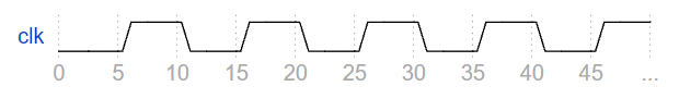
编写一个测试平台来创建模块dut 的一个实例(具有任何实例名称),并创建一个时钟信号来驱动模块的clk输入。时钟周期为 10 ps。时钟应初始化为零,其第一次转换为 0 到 1。
代码实现:
module top_module ( );

    reg clk;

    initial begin
        clk=1'b0;
    end

    always #5 clk = ~ clk;

    dut u0(clk);

endmodule
验证结果:
2、测试平台1
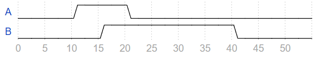
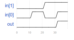
创建一个 Verilog 测试平台,将为输出 A 和 B 生成以下波形:
代码实现:
module top_module ( output reg A, output reg B );//

    // generate input patterns here
    initial begin
        A = 1'b0;
        B = 1'b0;
		#10 A=1;
        #5 B=1;
        #5 A=0;
        #20 B=0;
    end

endmodule
验证结果:
3、与门
您将获得以下要测试的 AND 门:
module andgate (
    input [1:0] in,
    output out
);
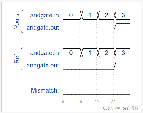
通过生成以下时序图,编写一个测试平台,实例化此与门并测试所有 4 个输入组合:
代码实现:
module top_module();

    reg [1:0] in,out;
    initial begin
            in = 2'b00;
            #10 in=2'b01;
            #10 in=2'b10;
            #10 in=2'b11;
    end

    andgate U0(.in(in), .out(out));

endmodule
验证结果:
4、测试平台2
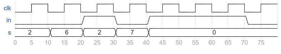
根据下面的波形设置clk、in和s:
模块 q7 具有以下声明:
module q7 (
    input clk,
    input in,
    input [2:0] s,
    output out
);
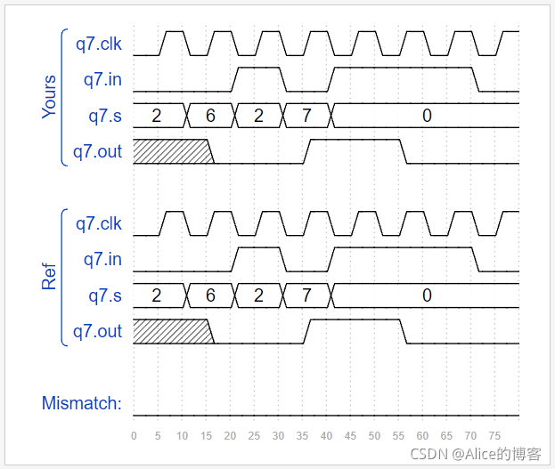
编写一个测试平台,实例化模块q7并完全如上图所示生成这些输入信号。
代码实现:
module top_module();

    reg clk,in,out;
    reg [2:0] s;

    initial begin
        clk=1'b0;
        s = 3'd2;
        in = 1'b0;
        #10 s = 3'd6;
        #10 begin
            s = 3'd2;
            in = 1'b1;
        end
        #10 begin
            s = 3'd7;
            in = 1'b0;
        end
        #10 begin
            s = 3'd0;
            in = 1'b1;
        end
        #30 in = 1'b0;
    end

    always #5 clk = ~ clk;

    q7 U0(.clk(clk), .in(in), .s(s), .out(out));

endmodule
验证结果:
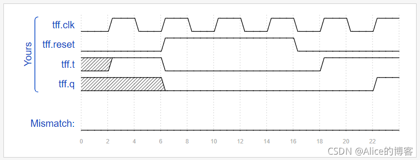
5、T 触发器
您将获得一个带有以下声明的 T 触发器模块:
module tff (
    input clk,
    input reset,   // active-high synchronous reset
    input t,       // toggle
    output q
);
编写一个测试平台,实例化一个tff并将重置 T 触发器,然后将其切换到“1”状态。
代码实现:
module top_module ();

    reg clk,reset,t,q;

    initial begin
        clk=1'b0;
        reset = 1'b0;
        #6 reset = 1'b1;
        #10 reset = 1'b0;
    end

    always #2 clk = ~ clk;

    always@(posedge clk) begin
        if(reset==1'b1)
            t <= 1'b0;
        else
            t <= 1'b1;
    end

    tff U0(.clk(clk), .reset(reset), .t(t), .q(q));

endmodule
验证结果:


 被折叠的 条评论
为什么被折叠?
被折叠的 条评论
为什么被折叠?
 到【灌水乐园】发言


