


 本文介绍了SRAM、DRAM和RLDRAM三种内存类型。SRAM速度快、功耗低但容量小;DRAM则具有大容量、低成本,但需要刷新以防止数据丢失。RLDRAM作为DRAM的一种,提供了更低的延迟和更高的带宽,适用于网络应用。内容还包含了QDR SRAM和RLDRAM的具体参数与性能比较。
SRAM:
Static RAM (SRAM) consists of flip-flops, a bistable circuit composed of four to six transistors. Once a flip-flop stores a bit, it keeps that value until the opposite value is stored in it.
SRAM CELL: Vertical: bit line. Horizontal: word line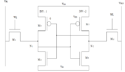
DRAM:
Dynamic random-access memory
SRAM: is a memory chip that is faster, smaller and uses less power than DRAM.
DRAM: is a memory chip that can hold more data than an SRAM chip, has large cpacity and also cheaper, but it requires more power. As time passes, the charges in the memory cells leak away, so it needs to be refreshed to prevent the stored data from being lost
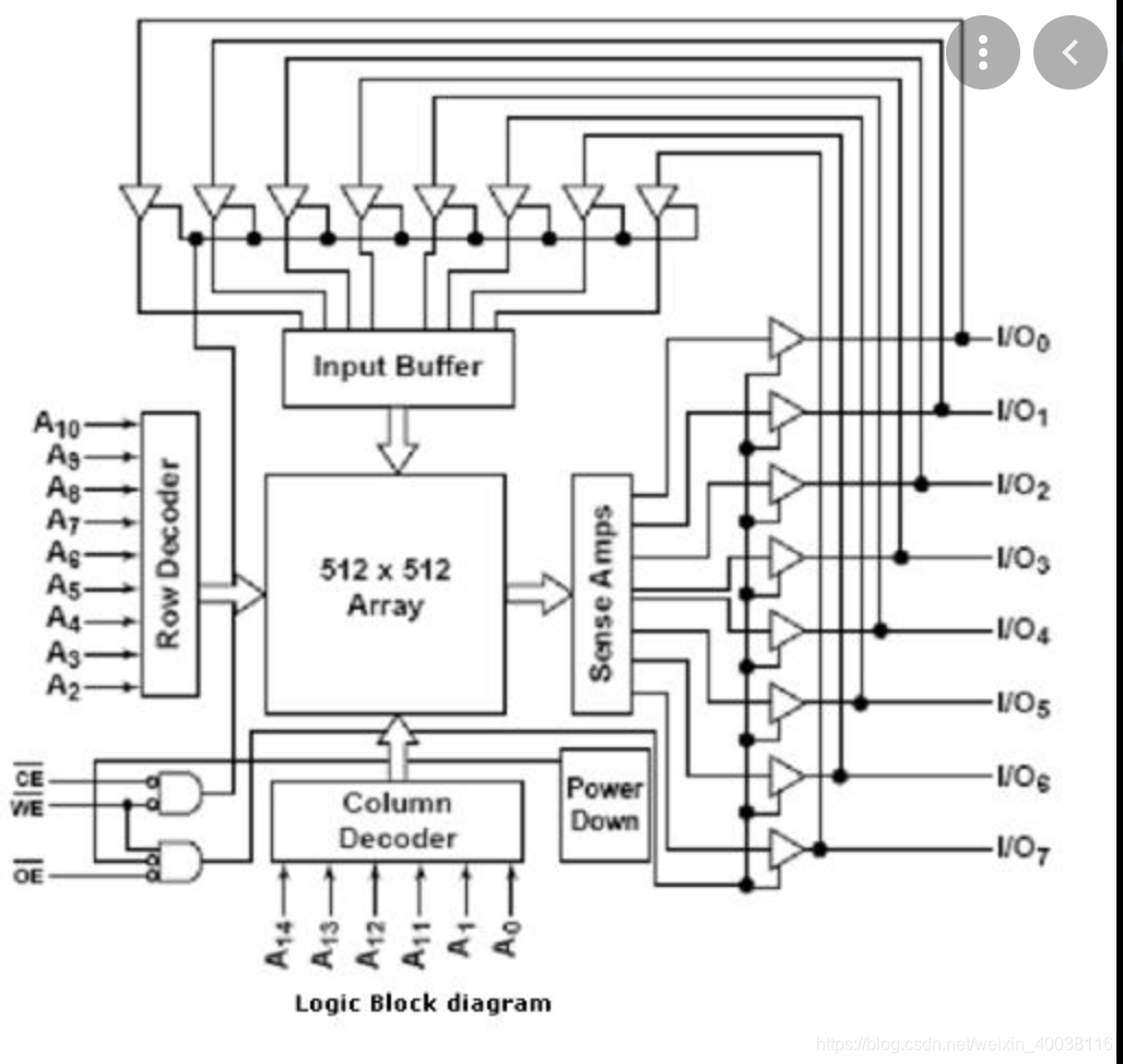
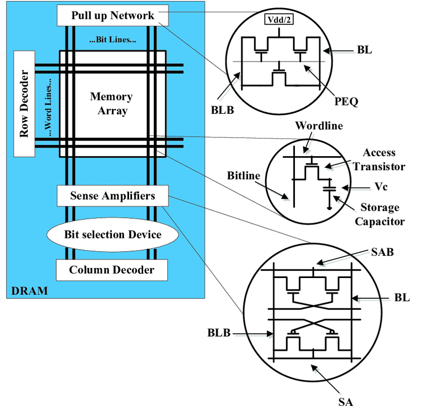
The sense amplifier in above memory is part of the read circuitry that is used when data is read from the memory; its role is to sense the low power signals from a bitline that represents a data bit (1 or 0) stored in a memory cell, and amplify the small voltage swing to recognizable logic levels so the data can be interpreted properly
RLDRAM
Definition:
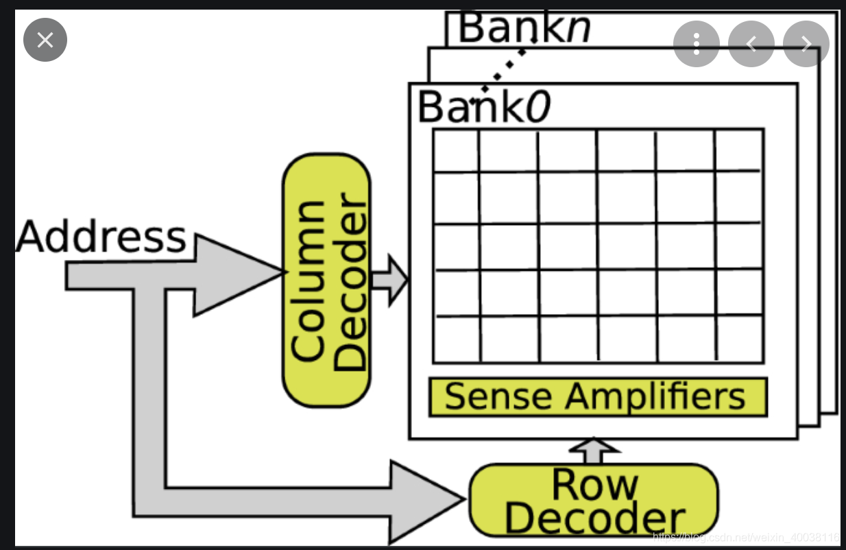
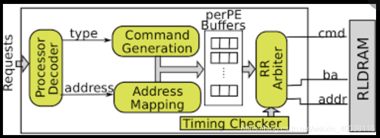
- Reduced Latency DRAM is one sepcial kind of DRAM, which uses the same internal memory array in DRAMs is organized as “banks,” with a memory location specified in the form of bank, row, and column addresses.
- The RLDRAM II has an SRAM-like interface that makes it more suitable for networking applications than other DRAMs. The addressing of the device is similar to that of an SRAM—address supplied does not have to be in the form of row address and column address as is the case with standard DRAMs. In typical DRAMs, row activation needs to occur before a column address is provided, thereby making the array access a two-step process. In RLDRAM, with internal precharge and built-in activation, the entire addressing is done in a single cycle, which makes addressing much simpler.
- RLDRAM II is equipped with double data rate interfaces that allow data to be transferred on both the rising and falling edges of the clock, thereby doubling the bandwidth compared to the standard single data rate interface.
- While typical commodity DRAM architectures have four banks, the RLDRAM has eight banks. This allows for shorter column/row address and data bit lines, resulting in a faster access time.
There also two kinds of memories that is used today:
SDRAM: Synchronous dynamic RAM need to refresh, with fast speed and large capacity.
DDR SDRAM: Dual-channel synchronous dynamic RAM, requires refreshing, with fast speed and large capacity.
Two memoris I've been using recently
QDR SRAM:
addr width: 19 bits
data width: 36 bits
burst length (configurable): 4
effective data width (based on burst length): 144 bits
operating frequency: 400 MHz
read latency: 2.5 cc
write latency: 1 cc
RLDRAM:
addr width: 19 bits
data width: 72 bits
burst length (configurable): 4
effective data width (based on burst length): 144 bits
operating frequency: 2133 MHz (recently changed from 2400 MHz)
read latency: 19 cc
write latency: 18 cc
Example of QDR & RLDRAM initialization (Verilog)
qdr2 qdr2 (
    // Outputs
    .mem_d           (QDR_D),
    .mem_wps_n       (QDR_W_N),
    .mem_bws_n       (QDR_BW_N),
    .mem_a           (QDR_SA),
    .mem_rps_n       (QDR_R_N),
    .mem_k           (QDR_K_P),
    .mem_k_n         (QDR_K_N),
    .mem_doff_n      (QDR_DLL_OFF_N),
    .afi_clk         (qdr_clk),
    .afi_half_clk    (),
    .afi_reset_n     (qdr_reset_n),
    .avl_w_ready     (qdr_w_ready),
    .avl_r_ready     (qdr_r_ready),
    .avl_r_rdata_valid   (qdrReadValid),
    .avl_r_rdata         (qdrDataRead),
    .local_init_done     (local_init_done),
    .local_cal_success   (local_cal_success),
    .local_cal_fail      (local_cal_fail),
    // Inputs
    .mem_q       (QDR_Q),
    .mem_cq      (QDR_CQ_P),
    .mem_cq_n        (QDR_CQ_N),
    .pll_ref_clk     (CLK_100_P[1]),
    .global_reset_n  (RESET_N),
    .soft_reset_n    (RESET_N),
    .avl_w_write_req (qdrWrite),
    .avl_w_addr      (qdrAddressWrite),
    .avl_w_size      (avl_w_size),
    .avl_w_wdata     (qdrDataWrite),
    .avl_r_read_req  (qdrRead),
    .avl_r_addr      (qdrAddressRead),
    .avl_r_size      (avl_r_size),
    .oct_rzqin       (QDR_RZQ)
);
Reference:
https://www.intel.com/content/dam/www/programmable/us/en/pdfs/literature/wp/wp_memoryselect.pdf


 957
957

 被折叠的 条评论
为什么被折叠?
被折叠的 条评论
为什么被折叠?
 到【灌水乐园】发言


