


 本文介绍了一种使用PMOS晶体管实现TPS61170升压转换器输入到输出隔离的方法,即负载断开功能。通过在设备禁用时断开输入电压与输出电压之间的连接,确保了电源与负载的有效隔离。
http://www.ti.com/lit/an/slva299a/slva299a.pdf
Many boost converters have an external rectifier diode.
The input voltage of the TPS61170 main boost converter is connected to the output voltage when the device is disabled.
Due to the direct pass from the input to the output, the input supply is not isolated from the output voltage when the IC is disabled.
This application report describes how to use a PMOS transistor to disconnect the boost converter’s input voltage from the output voltage
(known as load disconnect or input to output isolation) when the device is disabled.
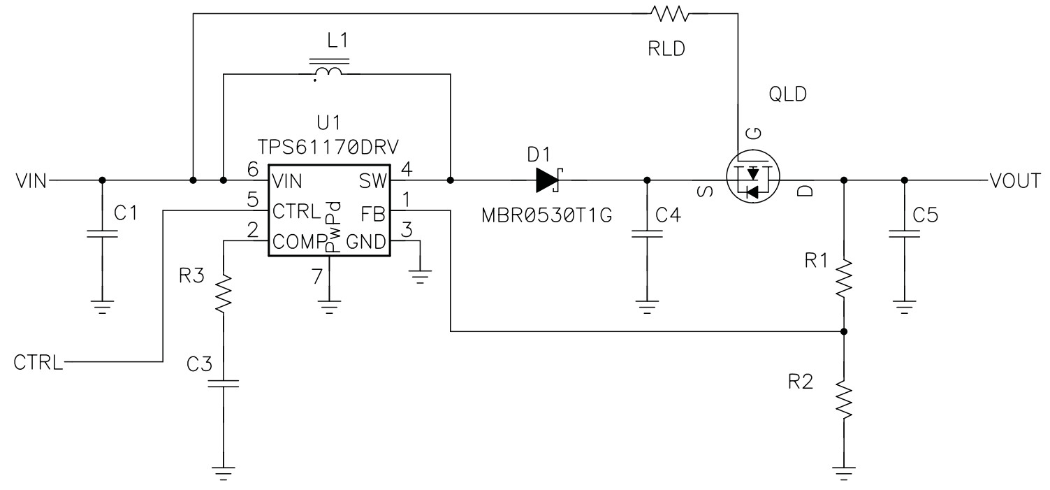
Figure 1 shows the schematic for a TPS61170EVM (SLVU222) that has been modified to include a PMOS transistor Q(LD), and a resistor R(LD)
which form the load disconnect circuit. Capacitor C4 is the minimum capacitor necessary for control loop stability, and C5 represents additional load capacitance.
The boost converter's diode is connected to the source of Q(LD), but the feedback network and output capacitor are connected after Q(LD).
This allows a regulated output voltage even with the use of the transistor Q(LD).
Select Q(LD) to have the following characteristics:
1. a VSD breakdown voltage higher than VOUT
2. a VGS breakdown voltage higher than VOUT – VINmin
3. a low drain to source resistance (RDS(on)) such that the voltage drop created by the maximum output current (IOmax) times RDS(on)
does not take the output voltage below the required minimum regulated voltage for the application.
Capacitor C4 provides a defined bias operation point for Q(LD) and can should be in the 0.1uF to 1uF range.
R(LD)of approximately 100 Ω is recommended to prevent the input voltage from capacitively coupling to the boost converter output.
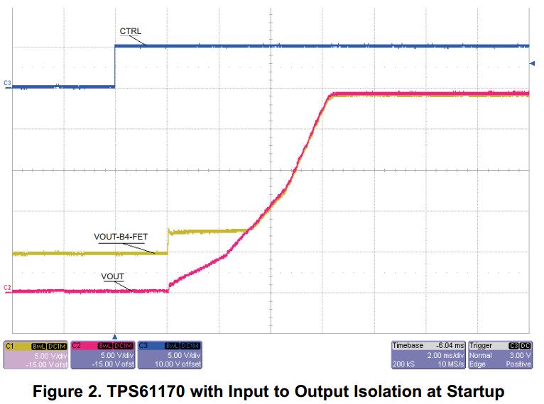
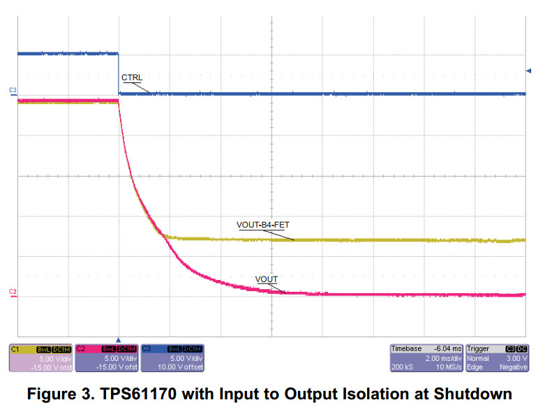
UsingFigure 1 with VIN = 5V and VOUT set to 24 V by R1 and R2, and RLOAD = 240 Ω (IOUT = 100 mA),
Figure 2 shows the circuit starting up while Figure 3 shows the circuit at shutdown.
In both figures, CH1 shown in yellow and set to 5 V/div, shows output voltage before Q(LD) ,
CH2 shown in pink and set to 5 V/div, shows the output voltage after Q(LD), and
CH3 shown in blue, shows CTRL.
Note that the load regulation at large loads is degraded by the IOUT × RDS(on) drop across the FET, i.e.,
VOUT = VREF × (1 + R1/R2) – IOUT × RDS(on).
Note also that efficiency will be degraded slightly due to the IOUT 2 × RDS(on) additional power loss across the FET,
i.e. η = ((VREF × (1 + R1/R2) – IOUT × RDS(on)) × IOUT)/(VIN × IIN).
In this example, the Si2343 -30-V PFET with RDS(on)= 45 mΩ at VGS = 10V was used.
So, with VIN = 12V, the change in load regulation and efficiency is negligible.
At lower input voltages, higher currents, or when using FETs with higher RDS(on), the degradation in load regulation and efficiency is more apparent.


 321
321

 被折叠的 条评论
为什么被折叠?
被折叠的 条评论
为什么被折叠?
 到【灌水乐园】发言


