


 本文介绍了如何将德州仪器(TI)的DSP程序从RAM模式转换为FLASH模式,确保程序在电源断电后仍能保留。关键步骤包括替换链接器配置文件(F28335.cmd),添加必要的初始化代码,并在CCS中调整工程设置。程序在启动时会自动将关键代码段复制到RAM中执行,保证了程序的稳定运行。
在前面章节那些实验我们都是将程序烧写到芯片 RAM 中运行调试的,我们知道 RAM 中存储的东西在掉电后是会丢失的,也就是说程序烧入到 RAM 中运行,如
果系统电源关闭后再开启,之前下载的程序是不会再运行的。如果我们做好的产
品给客户不可能还让客户像我们这样使用 DSP 仿真器去烧录程序运行,所以非常
有必要学习如何将程序烧入到芯片 FLASH 中,这样即使掉电也不会丢失。
1 配置成 FLASH 模式步骤
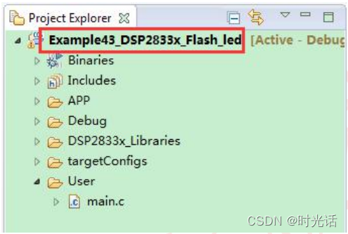
①将前面定时器实验章节的程序“Example24_DSP2833x_SCI_echoback”复制一份,重新命名为“Example43_DSP2833x_Flash_led”。
②打开 CCS 软件,导入工程“Example43_DSP2833x_Flash_led”,并将 CCS软件工程名修改为实验名称,这个在最开始实验章节就有介绍。如下所示:
③将工程目录“DSP2833x_Libraries”下的 28335_RAM_lnk.cmd 删除,然后 从 TI 提供 给我 们的 库文件 中把 “ F28335.cmd” 拷贝 到现 在实 验文件 夹 “DSP2833x_Libraries”目录下。如下:
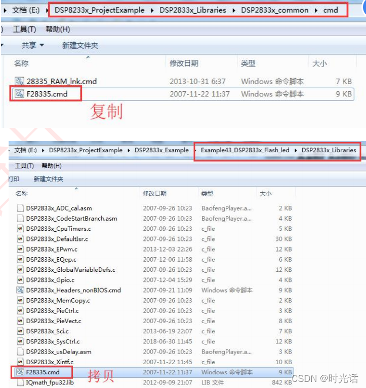
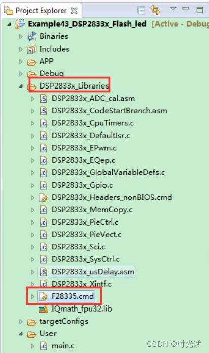
在工程目录下自动将“F28335.cmd”文件更新进来,如下:
该文件是对 FLASH 模式的配置,TI 公司已经给我们配置好了,一般我们不需要更改。
④在 main 函数开始处添加 FLASH 模式配置的必须代码,如下:
//复制对时间敏感代码和 FLASH 配置代码到 RAM 中
// 包括 FLASH 初始化函数 InitFlash();
// 链 接 后 将 产 生 RamfuncsLoadStart, RamfuncsLoadEnd, 和 RamfuncsRunStart
// 参数. 请参考 F28335.cmd 文件
MemCopy(&RamfuncsLoadStart, &RamfuncsLoadEnd, &RamfuncsRunStart);
// 调用 FLASH 初始化函数来设置 flash 等待状态
// 这个函数必须在 RAM 中运行
InitFlash();
上述两条语句是在使用 FLASH 模式必要的,通过这两条语句以及 F28335.cmd文件即可将程序烧入到芯片的 FLASH 中,这样程序断电后也不会丢失。
至此,我们就介绍完了如何将 RAM 调试程序修改成 FLASH 程序,大家只要按
照上述步骤完成即可,重点是第 3、4 步。
2 软件设计
(1)F28335.cmd
/*
// TI File $Revision: /main/9 $
// Checkin $Date: August 28, 2007   11:23:38 $
//###########################################################################
//
// FILE:	F28335.cmd
//
// TITLE:	Linker Command File For F28335 Device
//
//###########################################################################
// $TI Release: DSP2833x Header Files V1.01 $
// $Release Date: September 26, 2007 $
//###########################################################################
*/

/* ======================================================
// For Code Composer Studio V2.2 and later
// ---------------------------------------
// In addition to this memory linker command file,
// add the header linker command file directly to the project.
// The header linker command file is required to link the
// peripheral structures to the proper locations within
// the memory map.
//
// The header linker files are found in <base>\DSP2833x_Headers\cmd
//
// For BIOS applications add:      DSP2833x_Headers_BIOS.cmd
// For nonBIOS applications add:   DSP2833x_Headers_nonBIOS.cmd
========================================================= */

/* ======================================================
// For Code Composer Studio prior to V2.2
// --------------------------------------
// 1) Use one of the following -l statements to include the
// header linker command file in the project. The header linker
// file is required to link the peripheral structures to the proper
// locations within the memory map                                    */

/* Uncomment this line to include file only for non-BIOS applications */
/* -l DSP2833x_Headers_nonBIOS.cmd */

/* Uncomment this line to include file only for BIOS applications */
/* -l DSP2833x_Headers_BIOS.cmd */

/* 2) In your project add the path to <base>\DSP2833x_headers\cmd to the
   library search path under project->build options, linker tab,
   library search path (-i).
/*========================================================= */

/* Define the memory block start/length for the F28335
   PAGE 0 will be used to organize program sections
   PAGE 1 will be used to organize data sections

    Notes:
          Memory blocks on F28335 are uniform (ie same
          physical memory) in both PAGE 0 and PAGE 1.
          That is the same memory region should not be
          defined for both PAGE 0 and PAGE 1.
          Doing so will result in corruption of program
          and/or data.

          L0/L1/L2 and L3 memory blocks are mirrored - that is
          they can be accessed in high memory or low memory.
          For simplicity only one instance is used in this
          linker file.

          Contiguous SARAM memory blocks can be combined
          if required to create a larger memory block.
 */


MEMORY
{
PAGE 0:    /* Program Memory */
           /* Memory (RAM/FLASH/OTP) blocks can be moved to PAGE1 for data allocation */

   ZONE0       : origin = 0x004000, length = 0x001000     /* XINTF zone 0 */
   RAML0       : origin = 0x008000, length = 0x001000     /* on-chip RAM block L0 */
   RAML1       : origin = 0x009000, length = 0x001000     /* on-chip RAM block L1 */
   RAML2       : origin = 0x00A000, length = 0x001000     /* on-chip RAM block L2 */
   RAML3       : origin = 0x00B000, length = 0x001000     /* on-chip RAM block L3 */
   ZONE6A      : origin = 0x100000, length = 0x00FC00    /* XINTF zone 6 - program space*/
   ZONE7       : origin = 0x200000, length = 0x100000    /* XINTF zone 7  */
   FLASHH      : origin = 0x300000, length = 0x008000     /* on-chip FLASH */
   FLASHG      : origin = 0x308000, length = 0x008000     /* on-chip FLASH */
   FLASHF      : origin = 0x310000, length = 0x008000     /* on-chip FLASH */
   FLASHE      : origin = 0x318000, length = 0x008000     /* on-chip FLASH */
   FLASHD      : origin = 0x320000, length = 0x008000     /* on-chip FLASH */
   FLASHC      : origin = 0x328000, length = 0x008000     /* on-chip FLASH */
   FLASHA      : origin = 0x338000, length = 0x007F80     /* on-chip FLASH */
   CSM_RSVD    : origin = 0x33FF80, length = 0x000076     /* Part of FLASHA.  Program with all 0x0000 when CSM is in use. */
   BEGIN       : origin = 0x33FFF6, length = 0x000002     /* Part of FLASHA.  Used for "boot to Flash" bootloader mode. */
   CSM_PWL     : origin = 0x33FFF8, length = 0x000008     /* Part of FLASHA.  CSM password locations in FLASHA */
   OTP         : origin = 0x380400, length = 0x000400     /* on-chip OTP */
   ADC_CAL     : origin = 0x380080, length = 0x000009     /* ADC_cal function in Reserved memory */

   IQTABLES    : origin = 0x3FE000, length = 0x000b50     /* IQ Math Tables in Boot ROM */
   IQTABLES2   : origin = 0x3FEB50, length = 0x00008c     /* IQ Math Tables in Boot ROM */
   FPUTABLES   : origin = 0x3FEBDC, length = 0x0006A0     /* FPU Tables in Boot ROM */
   ROM         : origin = 0x3FF27C, length = 0x000D44     /* Boot ROM */
   RESET       : origin = 0x3FFFC0, length = 0x000002     /* part of boot ROM  */
   VECTORS     : origin = 0x3FFFC2, length = 0x00003E     /* part of boot ROM  */

PAGE 1 :   /* Data Memory */
           /* Memory (RAM/FLASH/OTP) blocks can be moved to PAGE0 for program allocation */
           /* Registers remain on PAGE1                                                  */

   BOOT_RSVD   : origin = 0x000000, length = 0x000050     /* Part of M0, BOOT rom will use this for stack */
   RAMM0       : origin = 0x000050, length = 0x0003B0     /* on-chip RAM block M0 */
   RAMM1       : origin = 0x000400, length = 0x000400     /* on-chip RAM block M1 */
   RAML4       : origin = 0x00C000, length = 0x001000     /* on-chip RAM block L1 */
   RAML5       : origin = 0x00D000, length = 0x001000     /* on-chip RAM block L1 */
   RAML6       : origin = 0x00E000, length = 0x001000     /* on-chip RAM block L1 */
   RAML7       : origin = 0x00F000, length = 0x001000     /* on-chip RAM block L1 */
   ZONE6B      : origin = 0x10FC00, length = 0x000400     /* XINTF zone 6 - data space */
   FLASHB      : origin = 0x330000, length = 0x008000     /* on-chip FLASH */
}

/* Allocate sections to memory blocks.
   Note:
         codestart user defined section in DSP28_CodeStartBranch.asm used to redirect code
                   execution when booting to flash
         ramfuncs  user defined section to store functions that will be copied from Flash into RAM
*/

SECTIONS
{

   /* Allocate program areas: */
   .cinit              : > FLASHA      PAGE = 0
   .pinit              : > FLASHA,     PAGE = 0
   .text               : > FLASHA      PAGE = 0
   codestart           : > BEGIN       PAGE = 0
   ramfuncs            : LOAD = FLASHD,
                         RUN = RAML0,
                         LOAD_START(_RamfuncsLoadStart),
                         LOAD_END(_RamfuncsLoadEnd),
                         RUN_START(_RamfuncsRunStart),
                         PAGE = 0

   csmpasswds          : > CSM_PWL     PAGE = 0
   csm_rsvd            : > CSM_RSVD    PAGE = 0

   /* Allocate uninitalized data sections: */
   .stack              : > RAMM1       PAGE = 1
   .ebss               : > RAML4       PAGE = 1
   .esysmem            : > RAMM1       PAGE = 1

   /* Initalized sections go in Flash */
   /* For SDFlash to program these, they must be allocated to page 0 */
   .econst             : > FLASHA      PAGE = 0
   .switch             : > FLASHA      PAGE = 0

   /* Allocate IQ math areas: */
   IQmath              : > FLASHC      PAGE = 0                  /* Math Code */
   IQmathTables     : > IQTABLES,  PAGE = 0, TYPE = NOLOAD
   IQmathTables2    : > IQTABLES2, PAGE = 0, TYPE = NOLOAD
   FPUmathTables    : > FPUTABLES, PAGE = 0, TYPE = NOLOAD

   /* Allocate DMA-accessible RAM sections: */
   DMARAML4         : > RAML4,     PAGE = 1
   DMARAML5         : > RAML5,     PAGE = 1
   DMARAML6         : > RAML6,     PAGE = 1
   DMARAML7         : > RAML7,     PAGE = 1

   /* Allocate 0x400 of XINTF Zone 6 to storing data */
   ZONE6DATA        : > ZONE6B,    PAGE = 1

   /* .reset is a standard section used by the compiler.  It contains the */
   /* the address of the start of _c_int00 for C Code.   /*
   /* When using the boot ROM this section and the CPU vector */
   /* table is not needed.  Thus the default type is set here to  */
   /* DSECT  */
   .reset              : > RESET,      PAGE = 0, TYPE = DSECT
   vectors             : > VECTORS     PAGE = 0, TYPE = DSECT

   /* Allocate ADC_cal function (pre-programmed by factory into TI reserved memory) */
   .adc_cal     : load = ADC_CAL,   PAGE = 0, TYPE = NOLOAD

}

/*
//===========================================================================
// End of file.
//===========================================================================
*/
void MemCopy(Uint16 *SourceAddr, Uint16* SourceEndAddr, Uint16* DestAddr)
{
    while(SourceAddr < SourceEndAddr)
    {
       *DestAddr++ = *SourceAddr++;
    }
    return;
}

void InitFlash(void)
{
   EALLOW;
   //Enable Flash Pipeline mode to improve performance
   //of code executed from Flash.
   FlashRegs.FOPT.bit.ENPIPE = 1;

   //                CAUTION
   //Minimum waitstates required for the flash operating
   //at a given CPU rate must be characterized by TI.
   //Refer to the datasheet for the latest information.
#if CPU_FRQ_150MHZ
   //Set the Paged Waitstate for the Flash
   FlashRegs.FBANKWAIT.bit.PAGEWAIT = 5;

   //Set the Random Waitstate for the Flash
   FlashRegs.FBANKWAIT.bit.RANDWAIT = 5;

   //Set the Waitstate for the OTP
   FlashRegs.FOTPWAIT.bit.OTPWAIT = 8;
#endif

#if CPU_FRQ_100MHZ
   //Set the Paged Waitstate for the Flash
   FlashRegs.FBANKWAIT.bit.PAGEWAIT = 3;

   //Set the Random Waitstate for the Flash
   FlashRegs.FBANKWAIT.bit.RANDWAIT = 3;

   //Set the Waitstate for the OTP
   FlashRegs.FOTPWAIT.bit.OTPWAIT = 5;
#endif
   //                CAUTION
   //ONLY THE DEFAULT VALUE FOR THESE 2 REGISTERS SHOULD BE USED
   FlashRegs.FSTDBYWAIT.bit.STDBYWAIT = 0x01FF;
   FlashRegs.FACTIVEWAIT.bit.ACTIVEWAIT = 0x01FF;
   EDIS;

   //Force a pipeline flush to ensure that the write to
   //the last register configured occurs before returning.

   asm(" RPT #7 || NOP");
}

void main()
{
	Uint16 p=0;


	InitSysCtrl();
	InitPieCtrl();
	IER = 0x0000;
	IFR = 0x0000;
	InitPieVectTable();

	//复制对时间敏感代码和FLASH配置代码到RAM中
	// 包括FLASH初始化函数 InitFlash();
	// 链接后将产生 RamfuncsLoadStart, RamfuncsLoadEnd, 和RamfuncsRunStart
	// 参数. 请参考 F28335.cmd 文件
	MemCopy(&RamfuncsLoadStart, &RamfuncsLoadEnd, &RamfuncsRunStart);
	// 调用FLASH初始化函数来设置flash等待状态
	// 这个函数必须在RAM中运行
	InitFlash();

	LED_Init();
	TIM0_Init(150,200000);//200ms
	UARTa_Init(4800);

	while(1)
	{
		p++;
				if((p%2)==0)
				 {
					LED2_TOGGLE;
				 }
				delay();
	}
}


 3126
3126

 被折叠的 条评论
为什么被折叠?
被折叠的 条评论
为什么被折叠?
 到【灌水乐园】发言


