


 本文详细解释了运算放大器在不同电源配置下的电压范围,包括总电源电压范围、输入共模电压范围和输出电压范围。通过实际例子展示了如何选择合适的运算放大器来满足电路需求。
http://e2e.ti.com/blogs_/archives/b/thesignal/archive/2012/05/08/op-amp-voltage-ranges-input-and-output-clearing-some-confusion.aspx
We often receive applications questions relating to the power supply, input and output voltage range capabilities of our op amps. It can be confusing so here is an attempt to sort it out:
First, common op amps don’t have ground terminals. A standard op amp does not “know” where ground is so it cannot know whether it is operating from a dual supply (±) or from a single power supply. As long as the power supply, input and output voltages are within their operating ranges, all is good.
Here are the three critical voltage ranges to consider:
- The total supply voltage range. This is total voltage between the two supply terminals. For example, ±15V is a total of 30V. The operating voltage range for an op amp might be, for example, 6V to 36V. At the low voltage extreme this could be ±3V or +6V. At maximum, ±18V or +36V or even ‑6V/+30V. Yes, unbalanced supplies are okay if you heed points 2 and 3 below.
- The input common-mode voltage range (C-M range) is generally specified relative to the positive and negative supply voltages, shown graphically in figure 1. In some equation-like form, C-M range of this hypothetical op amp would be described as 2V above the negative rail to 2.5V below the positive rail. Something like this… (V-)+2V to (V+)–2.5V.
- The output voltage range (or output swing capability) is. again, commonly specified relative to the rail voltages. In this case, (V-)+1V to (V+)–1.5V.
These examples (figures 1, 2, 3) are shown in a G=1 buffer configuration. A key point here… the output capability of this example in figure 1 will be limited to 2V from the negative rail and 2.5V from the positive rail and due to the limited input C-M range. This op amp would need to be configured in a higher gain to deliver its full output voltage range.

The example in Figure 1 is typical of an op amp generally used on dual ± supplies. It would not be called a “single supply” type but it certainly could be operated on a single supply just by staying within these ranges.
Figure 2 shows a so-called single supply op amp. It has a C-M range that extends to, and often slightly below the negative rail. This allows its use in a wider range of circuits that operate close to ground. So an op amp that is not called “single supply” could be used in some single supply circuits but a true single-supply type is more versatile in these applications.
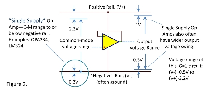
In this G=1 buffer circuit, this op amp would could produce an output swing of 0.5V from the V- rail (limited by output capability) and 2.2V from the V+ rails (limited by the input C-M range).
Figure 3 shows a “rail-to-rail” op amp. It can operate with input voltage equal to or even slightly beyond both supply voltage rails as shown in figure 3. Rail-to-rail output means that output voltage can swing very close to the rails, often within a 10mV to 100mV from the supply rails. Some op amps claim only a rail-to-rail output, lacking the input characteristics shown in figure 3. Rail-to-rail op amps are very commonly used on single 5V supplies and lower because they maximize signal voltage capability on their limited supply range.
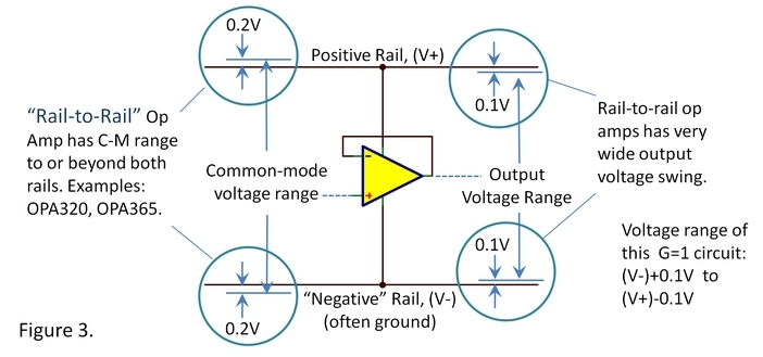
Rail-to-rail op amps are appealing because they ease signal voltage constraints but they are not always the best choice. Like other of life’s choices there are often tradeoffs with other performance attributes. But that’s why you are an analog designer. Your life is full of complex issues and tradeoffs and you love it!
Thanks for reading,
Bruce


 1万+
1万+

 被折叠的 条评论
为什么被折叠?
被折叠的 条评论
为什么被折叠?
 到【灌水乐园】发言


