National_Semiconductor的一款网络芯片的技术手册。1.0 Pin Descriptions
m
9
1.1 Serial Management Interface
9
1.2 MAC Data Interface
.9
1.3 Clock Interface
11
1. 4 LED Interface
1.5 Reset and Power down
12
1.6 Strap Options
12
1.7 10 Mb/s and 100 Mb/s PMD Interface
14
1.8 Special Connections
14
1. 9 Power Supply Pi
14
1. 10 Package Pin AsSi
15
2.0 Configuration
16
2. 1 Auto-Negotiation
g
16
2.1.1 Auto-Negotiation Pin Control
16
2.1.2 Auto-Negotiation Register Control
16
2.1.3 Auto-Negotiation Parallel Detection
2. 1. 4 Auto-Negotiation Restart
2.1.5 Enabling Auto-Negotiation via Software
17
2.1.6 Auto-Negotiation Complete Time
17
2.2 Auto-MDIX
2. 3 PHY Address
18
2.3.1 Mll Isolate mode
2.4 LED Interface
19
2.4.1LED
19
2.4.2 LED Direct Control
2.5 Half Duplex VS Full Duplex
20
2.6 Internal Loopback
20
2.7 BIST
20
3.0 Functional Description
.I.I...
21
3.1 Mll Interface
3.1.1 Nibble-wide mll data Interface
21
3.1.2 Collision detect
3.1.3 Carrier Sense
21
3.2 Reduced mll Interface
3.3 10 Mb Serial Network Interface(SNI)
.22
3. 4 802.3u Mll Serial Management Interface
3.4.1 Serial Management Register Access
3.4.2 Serial Management Access protocol
22
3.4.3 Serial Management Preamble Suppression
4.0 Architecture
24
4.1100BASE-TX TRANSMITTER
.24
4.1. 1 Code-group Encoding and Injection
26
4.1.2 Scrambler
26
4.1 3 Nrz to nrzi Encoder
26
4.1. 4 Binary to MLT-3 Convertor
26
4.2100 BASE-T×RECEⅣVER
26
4.2.1 Analog Front Et
26
4.2.2 Digital Signal Processor
26
4.2.2.1 Digital Adaptive Equalization and gain Control
28
4.2.2.2 Base Line Wander Compensation
4.2.3 Signal detect
4.2.4 MLT-3 to nrzi Decoder
4,25 nrz to nrz
4.2.6 Serial to parallel
4.2.7 Descrambler
4.2.8 Code-group Alignment
4.29 4B/5B Decoder
4.2. 10 100BASE-TX Link Integrity Monitor
..30
42. 11 Bad ssD Detection
.30
www.national.com
Oo寸∞∞∞
4.3 10BASE-T TRANSCEIVER MODULE
30
4.3.1 Operational Modes
30
4.3.2 Smart squelch
31
4.3.3 Collision Detection and sQE
4.3.4 Carrier Sense
31
4.3.5 Normal Link Pulse detection/Generation
4.3.6 Jabber function
…32
4.3. 7 Automatic Link Polarity detection and correction
.....32
4.3.8 Transmit and Receive Filtering
...32
4.3.9 Transmitter
4.3.10 Receiver
5.0 Design Guidelines
33
5. 1 TPI Network circuit
....33
5.2 ESD Protection
34
5.3 Clock In(X1) Requirements
34
5. 4 Power feedback circu
35
5.5 Power Down/Interrupt
35
5.5.1 Power down control mode
....35
5.5.2 Interrupt Mechanisms
5.6 Energy Detect Mode
36
6.0 Reset Operation..∴.∴∴∴.37
6.1 Hardware reset
6.2 Software reset
7.0 Register Block
,,,,,,,,,38
7. 1 Register definition
7.1.1 Basic Mode Control Register(BMCR)
7.1.2 Basic Mode Status Register(BMSR)
44
7.1.3 PHY Identifier Register #1 (PHYIDR1)
45
7.1. 4 PHY Identifier Register #2(PHYIDR2
..45
7.1.5 Auto-Negotiation Advertisement Register(ANAR)
.......45
7.1.6 Auto-Negotiation Link Partner Ability Register(ANLPAR) (BASE Page)
7.1.7 Auto-Negotiation Link Partner Ability Register(ANLPAR)(Next Page)
7.1.8 Auto-Negotiate Expansion Register (ANER)
7.1.9 Auto-Negotiation Next Page Transmit Register(ANNPTR)
7.2 EXtended Registers
50
7.2.1 PHY Status Register(PHYSTS
7.2.2 Mll Interrupt Control Register(MICR
52
7.2.3 MIl Interrupt Status and Misc. Control Register(MISR)
7.2.4 False Carrier Sense Counter Register(FCSCR)
7.2.5 Receiver Error Counter Register(RECR
7.2.6 100 Mb/s PCS Configuration and Status Register(PCSR)
55
7.2.7 RMII and Bypass Register(RBR)
7. 2. 8 LED Direct Control Register(LEDCR
7. 2. 9 PHY Control Register(PHYCR)
.....57
7.2.10 10Base-T Status/Control Register(1OBTSCR)
58
7. 2.11 CD Test and BIST Extensions Register(CDCTRL1)
60
7. 2. 12 Energy Detect Control (EDCR)
6
8.0 Electrical Specifications
62
8.1 DC Specs
62
8.2 AC Specs
.,,,,.,64
8.2.1 Power Up Timing
64
8.2.2 Reset Timing
8.2.3 Mll Serial Management Timing
8.2.4 100 Mb/s MIl Transmit Timing
8.2.5 100 Mb/s Mll Receive Timing
............67
8.2.6 100BASE-TX Transmit Packet Latency Timing
67
8.2.7 100BASE-TX Transmit Packet Deassertion Timing
8.2.8 100BASE-TX Transmit Timing(tr/F& Jitter)
8.2.9 100BASE-TX Receive Packet Latency Timing
70
8.2.10 100BASE-TX Receive Packet Deassertion Timing
70
www.national.com
8.2.11 10 Mb/s Mll Transmit Timing
71
8.2.12 10 Mb/s Mll Receive Timing
8.2.13 10 Mb/s serial Mode Transmit Timing
8.2.14 10 Mb/s serial Mode Receive timing
8.2.15 10BASE-T Transmit Timing (Start of Packet
73
8.2. 16 10BASE-T Transmit Timing(End of Packet
73
8. 2. 17 10BASE-T Receive Timing(Start of Packet)
8.2.18 10BASE-T Receive Timing(End of Packet
74
8.2.19 10 Mb/s heartbeat Timing
75
8.2.20 10 Mb/s Jabber Timing
8222 Auto-Negotiation Fast Link Pulse(FLP) Timing…、∴
8.2.21 10BASE-T Normal Link Pulse Timing
.....,,,,76
8.2.23 100BASE-TX Signal Detect Timing
8.2.24 100 Mb/s Internal loopback timing
8.2.25 10 Mb/s Internal Loopback Timing
.78
8. 2.26 RMII Transmit Timing
.79
8.2.27 RMII Receive Timing
82.28
Isolation Timing
81
8.2.29 25 MHz OUT Timing
81
8.2.30 100 Mb/s X1 to TX CLK Timing
82
9.0 Physical Dimensions∴∴
■■■
84
ww.national. com
Oo寸∞∞∞
List of Figures
Figure 1. DP83848C Functional Block Diagram.....
Figure 2. PHYAD Strapping Example
18
Figure 3. AN Strapping and LED Loading Example
19
Figure 4. Typical MDC/MDIO Read Operation
......23
Figure 5. Typical MDC/MDIO Write Operation
23
Figure 6. 100BASE-TX Transmit Block Diagram
,,,,,,.,,.24
Figure 7. 100BASE-TX Receive Block Diagram
27
Figure 8. EIA/TIA Attenuation Vs Frequency for 0, 50, 100, 130&150 meters of CAt 5 cable...... 28
Figure 9. 100BASE-TX BLW Event ........
Figure 10. 10BASE-T Twisted Pair Smart Squelch Operation
31
Figure 11 10/100 Mb/s Twisted Pair Interface...,..........
33
Figure 12. Crystal Oscillator Circuit
34
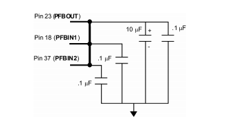
Figure 13. Power Feeback Connection
35
www.national.com
List of tables
Table 1. Auto-Negotiation Modes
.16
Table 2. PHY Address Mapping
Table 3. lEd Mode select
19
Table 4. Supported packet sizes at +/-50ppm +/-100ppm for each clock
Table 5. Typical MDIO Frame Format
Table 5. 4B5B Code-Group Encoding/Decoding
Table 6. 25
.,34
Table7.25 MHz Oscillator Specification∴.∴.∴
,,,,,,,,,,34
Table 8. 50 MHz Oscillator Specification
,,35
Table 9. 25 MHz Crystal Specification
Table 10 Register Map......................
38
Table 11. Register Table
..∴......39
Table 12. Basic Mode Control Register (BMCR), address 0X00
Table 13. Basic Mode Status Register(BMSR), address 0x01
Tabe14. PHY ldentifier Register#1( PHYIDR1), address0x02.∴………………………4
Table 15 PHY Identifier Register #2 (PHYIDR2), address 0x03
45
Table 16. Negotiation Advertisement Register(ANAR), address 0x04
45
Table 17. Auto-Negotiation Link Partner Ability Register(ANLPAR)(BASE Page), address 0x05.... 46
Table 18 Auto-Negotiation Link Partner Ability Register(ANLPAR)(Next Page), address 0x05..... 48
Table 19. Auto-Negotiate Expansion Register(ANER), address 0X06
Table 20 Auto-Negotiation Next Page Transmit Register(ANNPTR), address 0x07
.∴.∴......,49
Table 21. PHY Status Register(PHYSTS), address 0x10
Table 22 Mll Interrupt Control Register(MICR), address 0x11
n..52
Table 23. MIl Interrupt Status and Misc. Control Register(MISR), address 0x12
.....∴.53
Table 24. False Carrier Sense Counter Register(FCSCR), address 0x14
54
Table 25 Receiver Error Counter Register(RECR), address 0x15
54
Table 26. 100 Mb/s PCS Configuration and Status Register(PCSR), address 0x16
Table 27. RMI and Bypass Register(RBR), addresses 0x17...................56
Table 28 LED Direct Control Register (LEDCR), address 0X18
量重面
重重m
56
Table 29 PHY Control Register(PHYCR), address Ox19
57
Table 30 10Base-T Status/Control Register(10BTSCR), address OX1A
Table 31. CD Test and BIST Extensions Register(CDCTRL1), address 0x1B
..60
Table 32. Energy Detect Control (EDCR), address 0x1D
,,61
www.national.com
Oo寸∞∞∞
In Layou
乙uzoOHOau
PFBIN2
24
RBIAS
23上 PFBOU
RX DV/MIL MODE
AVDD33
CRS/CRS DV/LED CFG
RESERVED
RX ER/MDIX EN
41
RESERVED
42
RXD O/PHYAD1
DP838480
PFBIN1
RXD 1/PHYAD2
Td
RXD 2/PHYAD3
TD
RXD 3/PHYAD4
AGND
OGND
JOVDD33
Hz=z3oa
au>u
c
u>uOu
p vie
NS Package Number Vbh48A
www.national.com
1.0 Pin Descriptions
The DP83848C pins are classified into the following inter- All DP83848C signal pins are i/o cells regardless of the
face categories(each interface is described in the sections particular use. The definitions below define the functionality
that follow
of the l/O cells for each pin
Serial Management Interface
Input
MAC Data Interface
Output
Clock Interface
Type: I/o Input/Output
LED Interface
Type OD Open Drain
Reset and power down
Type: PD, PU Internal Pulldown/Pullup
Strap Options
Strapping Pin(All strap pins have weak in-
--10/100 Mb/s Pmd Interface
ternal pull-ups or pull-downs. If the default
Special Connect Pins
strap value is needed to be changed then an
external 2.2 k resistor should be used
Power and ground pins
Please see Section 1.6 for details.)
Note: Strapping pin option. Please see Section 1.6 for strap
definitions
1.1 Serial Management Interface
Signal Name
Tvpe
Pin t
Description
MDC
31
MANAGEMENT DATA CLOCK: Synchronous clock to the MDIo
management data input/output serial interface which may be
asynchronous to transmit and receive clocks. The maximum clock
rate is 25 Mhz with no minimum clock rate
MDIO
30 MANAGEMENT DATA l/O: Bi-directional management instruc
tion/data signal that may be sourced by the station management
entity or the PhY. This pin requires a 1.5k pullup resistor
1.2 MAC Data Interface
Signal name
Type
Pin t
Description
TX CLK
MII TRANSMIT CLOCK: 25 MHz Transmit clock output in 100
Mb/s mode or 2.5 MHz in 10 mb/s mode derived from the 25 mHz
reference clock
Unused in emil mode the device uses the x1 reference clock in
put as the 50 MHz reference for both transmit and receive
SNI TRANSMIT CLOCK: 10 MHZ Transmit clock output in 10 Mb
SNI mode. The MAc should source TX EN and TXdO using this
clock
TX EN
L PD
Mll TRANSMIT ENABLE: Active high input indicates the pres
ence of valid data inputs on TXD3: 0
RMII TRANSMIT ENABLE: Active high input indicates the pres-
ence of valid data on TXD[1: 0
SNI TRANSMIT ENABLE: Active high input indicates the pres-
ence of valid data on TXD 0
TXD 0
MII TRANSMIT DATA: Transmit data Mll input pins, TXD3: 0
TXD 1
3456
that accept data synchronous to the TX ClK (2.5 MHz in 10 Mb/s
mode or 25 MHz in 100 Mb/s mode)
TXD 2
RMII TRANSMIT DATA: Transmit data RMII input pins, TXD[1
TXD 3
S.L. PD
that accept data synchronous to the 50 MHz reference clock
SNI TRANSMIT DATA: Transmit data sNi input pin TXd 0, that
accept data synchronous to the TX CLK (10 MHz in 10 Mb/s sni
mode)
www.national.com
Oo寸∞∞∞
Signal name
Type
Pin #i
Description
RX CLK
38
MI RECEE CLOCK: Provides the 25 mhz recovered receive
clocks for 100 Mb/s mode and 2.5 MHz for 10 Mb/s mode
Unused in rmll mode the device uses the xl reference clock in
put as the 50 MHz reference for both transmit and receive
SNI RECEIVE CLOCK: Provides the 10 MHz recovered receive
clocks for 10 Mb/s sni mode
RXD∨
S.O. PD
MII RECEIVE DATA VALID: Asserted high to indicate that valid
data is present on the corresponding RXD[3: 0]. MIl mode by de
fault with internal pulldown
RMII Synchronous Receive Data Valid: This signal provides the
RMII Receive Data valid indication independent of carrier sense
This pin is not used in SNI mode
RX ER
S.O. PU
MIl RECEIVE ERROR: Asserted high synchronously to RX CLK
to indicate that an invalid symbol has been detected within a re
ceived packet in 100 Mb/s mode
RMII RECEIVE ERROR: Assert high synchronously to X1 when-
ever it detects a media error and rxdv is asserted in 100 mb/s
This pin is not required to be used by a mac, in either mil or rmll
mode, since the Phy is required to corrupt data on a receive error
This pin is not used in SNI mode
RXD O
S.O. PD
MII RECEIVE DATA: Nibble wide receive data signals driven syn
RXd 1
chronously to the rx clk, 25 Mhz for 100 Mb/s mode 2.5 MHZ
for 10 Mb/s mode ) RXD[3 0] signals contain valid data when
RXD 2
45
RX DV is asserted
RXD 3
46
RMII RECEIVE DATA: 2-bits receive data signals, RXD[1: 0], driv
en synchronously to the X1 clock, 50 MHZ
SNI RECEIVE DATA: Receive data signal, RXD 0, driven syn
chronously to the RX ClK RXd0 contains valid data when CRs
is asserted. RXD[3: 1] are not used in this mode
CRS/CRS DV
S.O. PU
MII CARRIER SENSE: Asserted high to indicate the receive me
dium is non idle
RMII CARRIER SENSE/RECEIVE DATA VALID: This signal
combines the rmll carrier and receive data valid indications
For a detailed description of this signal, see the RMII Specifica-
SNI CARRIER SENSE: Asserted high to indicate the receive me
dium is non -idle. It is used to frame valid receive data on the
RXD 0 signal
COL
S.O. PU
MI COLLISION DETECT: Asserted high to indicate detection of
a collision condition(simultaneous transmit and receive activity)
in 10 Mb/s and 100 Mb/s Half Duplex Modes
While in 10BASE-T Half Duplex mode with heartbeat enabled this
pin is also asserted for a duration of approximately 1 s at the end
of transmission to indicate heartbeat (SQE test
In Full duplex Mode, for 10 Mb/s or 100 Mb/s operation, this sig
nal is always logic 0. There is no heartbeat function during 10
Mb/s full duplex operation
RMII COLLISION DETECT: Per the RMll Specification, no COL
signal is required. The MAc will recover CRS from the CRS DV
signal and use that along with its tX en signal to determine col-
SNI COLLISION DETECT: Asserted high to indicate detection of
a collision condition(simultaneous transmit and receive activity)
in 10 Mb/s sni mode
www.national.com
10


 5170
5170

 被折叠的 条评论
为什么被折叠?
被折叠的 条评论
为什么被折叠?
 到【灌水乐园】发言


